INTERPHASE CORPORATION
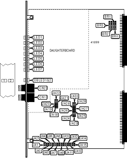
V/ATM 5215
|
NIC Type |
ATM (OC-3c) |
|
Processor |
Motorola 68EC040 |
|
Processor Speed |
20/25MHz |
|
Maximum Onboard Memory |
512KB SRAM/4MB SRAM |
|
Cache |
1024KB SRAM |
|
I/O Options |
Serial port (exact location and function unidentified) |
|
Boot ROM |
Not available |
|
Network Transfer Rate |
155Mbps |
|
Topology |
Unidentified |
|
Wire Type |
Fiber optic cable |
|
Data Bus |
VME double |

|
CONNECTIONS | |||
|
Function |
Label |
Function |
Label |
|
Fiber optic transmit cable connector |
CN1 |
Fiber optic receive cable connector |
CN2 |
|
USER CONFIGURABLE SETTINGS | |||
|
Setting |
Label |
Position | |
| » |
Power-on self-test enabled |
JA1 |
Open |
|
Power-on self-test disabled |
JA1 |
Closed | |
| » |
XON/XOFF flow control disabled |
JA2 |
Open |
|
XON/XOFF flow control enabled |
JA2 |
Closed | |
| » |
Factory configured - do not alter |
JA3 |
Open |
| » |
Factory configured - do not alter |
JA4 |
Open |
| » |
Factory configured - do not alter |
JA5 |
Open |
| » |
Serial port speed is 38.4K00bps |
JA6 |
Open |
|
Serial port speed is 9600bps |
JA6 |
Closed | |
| » |
Processor speed is 25MHz |
JA7 |
Open |
|
Processor speed is 20MHz |
JA7 |
Closed | |
| » |
Cache enabled |
JA8 |
Open |
|
Cache disabled |
JA8 |
Closed | |
| » |
Factory configured - do not alter |
JA9 |
Open |
| » |
Factory configured - do not alter |
JA10 |
Open |
| » |
Serial port disabled |
JA11 |
Open |
|
Serial port enabled |
JA11 |
Closed | |
| » |
GDB debug mode disabled |
JA12 |
Open |
|
GDB debug mode enabled |
JA12 |
Closed | |
| » |
DTACK signal not filtered |
JA13 |
Closed |
|
DTACK signal filtered |
JA13 |
Open | |
| » |
Card will request VME bus even when its request level is unavailable |
JA14 |
Open |
|
Card will not request VME bus until its request level is available |
JA14 |
Closed | |
| » |
Card will use standard release mode for releasing the VME bus |
JA15 |
Open |
|
Card will use early release mode for releasing the VME bus |
JA15 |
Closed | |
| » |
Short I/O size is 512 bytes |
JA18 |
Closed |
|
Short I/O size is 2048 bytes |
JA18 |
Open | |
| » |
VRAM buffer not accessible to VME A24 space |
JA19 |
Closed |
|
VRAM buffer is accessible to VME A24 space |
JA19 |
Open | |
| » |
VRAM allows non-privileged or privileged address modifiers |
JA20 |
Closed |
|
VRAM allows privileged address modifiers only |
JA20 |
Open | |
| » |
Factory configured - do not alter |
JA21 |
Open |
| » |
Factory configured - do not alter |
JA22 |
Open |
|
Short I/O compare circuitry to accept only privileged address modifiers |
JA23 |
Open | |
|
Short I/O compare circuitry to accept both privileged and non-privileged address modifiers. |
JA23 |
Closed | |
|
Note:The manufacturer suggests that JA18 remain closed. Not all boards may support VRAM buffer access in VME A24 space (jumper JA19). Contact the manufacturer for more information. If jumpers JA16 and JA17 are installed on your board they should remain open. | |||
|
INTERRUPT REQUEST PRIORITY SELECTION | ||||
|
Setting |
BR0 |
BR1 |
BR2 |
BR3 |
|
0 |
1 & 2, 3 & 4, 5 & 6 |
4 & 5 |
4 & 5 |
4 & 5 |
|
1 |
4 & 5 |
1 & 2, 3 & 4, 5 & 6 |
4 & 5 |
4 & 5 |
|
2 |
4 & 5 |
4 & 5 |
1 & 2, 3 & 4, 5 & 6 |
4 & 5 |
|
3 |
4 & 5 |
4 & 5 |
4 & 5 |
1 & 2, 3 & 4, 5 & 6 |
|
Note:Pins designated are in the closed position. | ||||
|
SHORT I/O BASE ADDRESS SELECTION | ||||||||
|
Setting |
JA24 |
JA25 |
JA26 |
JA27 |
JA28 |
JA29 |
JA30 | |
|
0000h |
Closed |
Closed |
Closed |
Closed |
Closed |
Closed |
Closed | |
|
0200h |
Closed |
Closed |
Closed |
Closed |
Closed |
Closed |
Open | |
|
0400h |
Closed |
Closed |
Closed |
Closed |
Closed |
Open |
Closed | |
|
0600h |
Closed |
Closed |
Closed |
Closed |
Closed |
Open |
Open | |
|
0800h |
Closed |
Open |
Open |
Closed |
Closed |
Closed |
Closed | |
| » |
6000h |
Closed |
Open |
Open |
Closed |
Closed |
Closed |
Closed |
|
F600h |
Open |
Open |
Open |
Open |
Closed |
Open |
Open | |
|
F800h |
Open |
Open |
Open |
Open |
Open |
Closed |
Closed | |
|
FA00h |
Open |
Open |
Open |
Open |
Open |
Closed |
Open | |
|
FC00h |
Open |
Open |
Open |
Open |
Open |
Open |
Closed | |
|
FE00h |
Open |
Open |
Open |
Open |
Open |
Open |
Open | |
|
Note: A total of 128 base address settings are available. The jumpers are a binary representation of the decimal memory addresses. JA24 is the Most Significant Bit and jumper JA30 is the Least Significant Bit. The jumpers have the following decimal values: JA24=32768, JA25=16384, JA26=8192, JA27=4096, JA28=2048, JA29=1024, JA30=512. Open the jumpers and add the values of the jumpers that are open to obtain the correct memory address. (Open=1, Closed=0) | ||||||||
|
DIAGNOSTIC LED(S) | |||||
|
LED1 Color |
LED1 Status |
LED5 Status |
LED6 Status |
LED7 Status |
Condition |
|
Red |
On |
Blinking |
Off |
Off |
Memory diagnostic test failed |
|
Red |
On |
Off |
Blinking |
Off |
DMA diagnostic test failed |
|
Red |
On |
Blinking |
Blinking |
Off |
FE diagnostic test failed |
|
Red |
On |
Off |
Off |
On |
Firmware panic condition occurred |
|
Red |
On |
On |
Off |
On |
VME bus error occurred |
|
Red |
On |
Off |
On |
On |
VME bus timeout occurred |
|
Red |
On |
Blinking |
Blinking |
Blinking |
Power-on reset in progress |
|
Red |
On |
On |
On |
On |
Power-on reset in progress |
|
Green |
On |
Blinking |
Blinking |
Blinking |
Common Boot Interface ready |
|
Green |
On |
Cycle |
Cycle |
Cycle |
Adapter is active |
|
N/A |
Off |
N/A |
N/A |
N/A |
Power is off or board is improperly installed |
|
DIAGNOSTIC LED(S) (CON'T) | |||
|
LED |
Color |
Status |
Condition |
|
LED2 |
Unidentified |
On |
Board is accessing SRAM |
|
LED2 |
Unidentified |
Off |
Board is not accessing SRAM |
|
LED3 |
Unidentified |
On |
Board is accessing VRAM |
|
LED3 |
Unidentified |
Off |
Board is not accessing VRAM |
|
LED4 |
Unidentified |
On |
VME bus is performing DMA transfer to board |
|
LED4 |
Unidentified |
Off |
VME bus is not performing DMA transfer to board |
|
DBLED1 |
Green |
On |
Network connection is good |
|
DBLED1 |
Green |
Off |
Network connection is broken |
|
DBLED2 |
Yellow |
On |
Power-on reset in progress |
|
DBLED2 |
Yellow |
Blinking |
Daughterboard is initialized and functioning |
|
DBLED2 |
Yellow |
Off |
Power-on reset complete |
|
Note:The term 'Cycle' in reference to LED5-LED7 indicated that the LEDs are turning on in sequence, one after the other. The colors of LED5-LED7 are unidentified. DBLED1 and DBLED2 are on the daughterboard. | |||