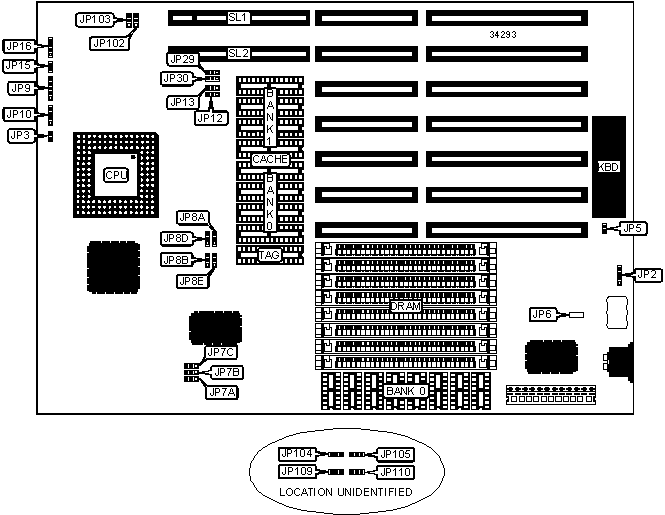
UNIDENTIFIED
486 VESA (REV. VL 421A/422)
|
Processor |
CX486S/80486SX/80487SX/80486DX/80486DX2/P24T |
|
Processor Speed |
20/25/33/40/50(internal)/50/66(internal)MHz |
|
Chip Set |
Forex |
|
Video Chip Set |
None |
|
Maximum Onboard Memory |
36MB |
|
Maximum Video Memory |
None |
|
Cache |
64/128/256KB |
|
BIOS |
AMI |
|
Dimensions |
330mm x 218mm |
|
I/O Options |
32-bit VESA local bus slots (2) |
|
NPU Options |
None |
|
CONNECTIONS | |||
|
Purpose |
Location |
Purpose |
Location |
|
External battery |
JP2 |
Turbo switch |
JP15 |
|
Reset switch |
JP3 |
Turbo LED |
JP16 |
|
Power LED & keylock |
JP9 |
32-bit VESA local bus slots |
SL1 & SL2 |
|
Speaker |
JP10 | ||
|
USER CONFIGURABLE SETTINGS | |||
|
Function |
Label |
Position | |
|
Battery type select internal |
JP2 |
Pins 1 & 2 closed | |
|
Battery type select external |
JP2 |
Closed | |
|
» |
Factory configured - do not alter |
JP5 |
Unidentified |
|
» |
Factory configured - do not alter (CMOS) |
JP6 |
Unidentified |
|
DRAM CONFIGURATION | |||
|
Size |
Bank 0 |
Bank 1 |
Bank 2 |
|
1MB |
None |
(4) 256K x 9 |
None |
|
2MB |
None |
(4) 256K x 9 |
(4) 256K x 9 |
|
4MB |
(8) 411000 |
None |
None |
|
4MB |
None |
(4) 1M x 9 |
None |
|
5MB |
(8) 411000 |
(4) 256K x 9 |
None |
|
5MB |
None |
(4) 1M x 9 |
(4) 256K x 9 |
|
8MB |
(8) 411000 |
(4) 1M x 9 |
None |
|
8MB |
None |
(4) 1M x 9 |
(4) 1M x 9 |
|
12MB |
(8) 411000 |
(4) 1M x 9 |
(4) 1M x 9 |
|
16MB |
None |
(4) 4M x 9 |
None |
|
20MB |
(8) 411000 |
(4) 4M x 9 |
None |
|
32MB |
None |
(4) 4M x 9 |
(4) 4M x 9 |
|
36MB |
(8) 411000 |
(4) 4M x 9 |
(4) 4M x 9 |
|
Note: The location of banks 1 & 2 are unidentified. | |||
|
DRAM JUMPER SELECTION | |
|
Setting |
JP105 |
|
DIPPs used as bank 0 |
Pins 1 & 2 closed |
|
SIMMs used as bank 0 |
Pins 2 & 3 closed |
|
CACHE CONFIGURATION | |||
|
Size |
Bank 0 |
Bank 1 |
TAG |
|
64KB |
(4) 8K x 8 |
(4) 8K x 8 |
(1) 8K x 8 |
|
128KB |
(4) 32K x 8 |
None |
(1) 8K x 8 |
|
256KB |
(4) 32K x 8 |
(4) 32K x 8 |
(1) 32K x 8 |
|
CACHE JUMPER CONFIGURATION | ||||
|
Size |
JP8A |
JP8B |
JP8D |
JP8E |
|
64KB |
Pins 2 & 3 closed |
Pins 2 & 3 closed |
Pins 2 & 3 closed |
Pins 2 & 3 closed |
|
128KB |
Pins 1 & 2 closed |
Pins 1 & 2 closed |
Pins 1 & 2 closed |
Pins 1 & 2 closed |
|
256KB |
Pins 2 & 3 closed |
Pins 1 & 2 closed |
Pins 2 & 3 closed |
Pins 1 & 2 closed |
|
CPU SPEED SELECTION | |||
|
Speed |
JP7A |
JP7B |
JP7C |
|
20MHz |
Pins 2 & 3 closed |
Pins 1 & 2 closed |
Pins 1 & 2 closed |
|
25MHz |
Pins 1 & 2 closed |
Pins 2 & 3 closed |
Pins 1 & 2 closed |
|
33MHz |
Pins 1 & 2 closed |
Pins 1 & 2 closed |
Pins 2 & 3 closed |
|
40MHz |
Pins 2 & 3 closed |
Pins 2 & 3 closed |
Pins 1 & 2 closed |
|
50iMHz |
Pins 1 & 2 closed |
Pins 2 & 3 closed |
Pins 1 & 2 closed |
|
50MHz |
Pins 2 & 3 closed |
Pins 1 & 2 closed |
Pins 2 & 3 closed |
|
66iMHz |
Pins 1 & 2 closed |
Pins 1 & 2 closed |
Pins 2 & 3 closed |
|
CPU TYPE SELECTION | |||
|
Type |
JP12 |
JP13 |
JP29 |
|
CX486S |
N/A |
N/A |
N/A |
|
80486 (PQFP) |
Pins 2 & 3 closed |
Pins 2 & 3 closed |
Pins 2 & 3 closed |
|
80486SX |
Pins 2 & 3 closed |
Pins 2 & 3 closed |
Pins 2 & 3 closed |
|
80487SX |
Pins 1 & 2 closed |
Pins 1 & 2 closed |
Pins 2 & 3 closed |
|
80486DX |
Pins 1 & 2 closed |
Pins 1 & 2 closed |
Pins 1 & 2 closed |
|
80486DX2 |
Pins 1 & 2 closed |
Pins 1 & 2 closed |
Pins 1 & 2 closed |
|
P24T |
N/A |
N/A |
N/A |
|
CPU TYPE SELECTION (CON’T) | ||||
|
Type |
JP30 |
JP104 |
JP109 |
JP110 |
|
CX486S |
N/A |
N/A |
N/A |
Pins 1 & 2 closed |
|
80486 (PQFP) |
Pins 2 & 3 closed |
N/A |
N/A |
N/A |
|
80486SX |
Pins 2 & 3 closed |
N/A |
N/A |
N/A |
|
80487SX |
Pins 2 & 3 closed |
N/A |
N/A |
N/A |
|
80486DX |
Pins 1 & 2 closed |
Pins 1 & 2 closed |
Pins 1 & 2 closed |
Pins 2 & 3 closed |
|
80486DX2 |
Pins 1 & 2 closed |
Pins 1 & 2 closed |
Pins 1 & 2 closed |
Pins 2 & 3 closed |
|
P24T |
N/A |
Pins 2 & 3 closed |
Pins 2 & 3 closed |
N/A |
|
VL BUS WAIT STATE SELECTION | ||
|
Setting |
JP102 |
JP103 |
|
0 |
Pins 1 & 2 closed |
Pins 1 & 2 closed |
|
1 |
Pins 2 & 3 closed |
Pins 2 & 3 closed |