INTEL CORPORATION
PD440FX
|
Processor |
Pentium II |
|
Processor Speed |
233/266MHz |
|
Chip Set |
Intel |
|
Video Chip Set |
None |
|
Maximum Onboard Memory |
256MB (EDO supported) |
|
Maximum Video Memory |
None |
|
Cache |
256/512KB |
|
BIOS |
AMI/Intel |
|
Dimensions |
288mm x 237mm |
|
I/O Options |
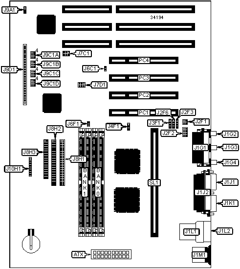
32-bit PCI slots (4), CD-ROM audio interface, floppy drive interface, game/MIDI port, green PC connector, IDE interfaces (2), parallel port, PS/2 mouse port, serial ports (2), CPU slot, IR connector, USB connectors (2), ATX power connector, telephony connectors (2), line in connectors (2), line out connector, microphone connector, wavetable connector, Yamaha wave table connectors (2) |
|
NPU Options |
None |
|
CONNECTIONS | |||
|
Purpose |
Location |
Purpose |
Location |
|
ATX power connector |
ATX |
IDE interface LED |
J6F1 |
|
Game/MIDI port |
J1G1 |
Yamaha wavetable connector |
J7C1 |
|
Microphone connector |
J1G2 |
Yamaha wavetable connector |
J7D1 |
|
Line in connector |
J1G3 |
IDE interface 1 |
J8H1 |
|
Line out connector |
J1G4 |
IDE interface 2 |
J8H2 |
|
Serial port 2 |
J1J1 |
Floppy drive interface |
J8H3 |
|
Parallel port |
J1J2 |
Chassis fan power |
J9A1 |
|
Serial port 1 |
J1K1 |
Soft off power |
J9D1 pins 1 & 2 |
|
USB connector 1 |
J1L1 |
Green PC connector |
J9D1 pins 3 & 4 |
|
USB connector 2 |
J1L2 |
IR connector |
J9D1 pins 6 - 11 |
|
PS/2 mouse port |
J1M1 |
IDE interface LED |
J9D1 pins 13 - 16 |
|
Telephony connector |
J2F1 |
Green PC LED |
J9D1 pins 18 - 20 |
|
Wavetable connector |
J2F2 |
Reset switch |
J9D1 pins 22 &23 |
|
Telephony connector |
J2F3 |
Speaker |
J9D1 pins 24 - 27 |
|
CD-ROM audio connector |
J2F6 |
GP I/O connector |
J10H1 |
|
Line in connector |
J3F1 |
32-bit PCI slots |
PC1 – PC4 |
|
Chassis fan power |
J4F1 |
Slot 1 processor connector |
SL1 |
|
Chassis security connector |
J6C1 | ||
|
USER CONFIGURABLE SETTINGS | |||
|
Function |
Label |
Position | |
|
» |
Flash BIOS normal operation |
J9C1A |
Pins 5 & 6 closed |
|
Flash BIOS recovery mode |
J9C1A |
Pins 4 & 5 closed | |
|
» |
CMOS memory normal operation |
J9C1C |
Pins 5 & 6 closed |
|
CMOS memory clear |
J9C1C |
Pins 4 & 5 closed | |
|
» |
Password enabled |
J9C1D |
Pins 1 & 2 closed |
|
Password disabled |
J9C1D |
Pins 2 & 3 closed | |
|
» |
Flash BIOS write protect disabled |
J9C1D |
Pins 5 & 6 closed |
|
Flash BIOS write protect enabled |
J9C1D |
Pins 4 & 5 closed | |
|
DRAM CONFIGURATION | ||
|
Size |
Bank 0 |
Bank 1 |
|
8MB |
(2) 1M x 36 |
None |
|
16MB |
(2) 2M x 36 |
None |
|
16MB |
(2) 1M x 36 |
(2) 1M x 36 |
|
24MB |
(2) 2M x 36 |
(2) 1M x 36 |
|
32MB |
(2) 4M x 36 |
None |
|
32MB |
(2) 2M x 36 |
(2) 2M x 36 |
|
40MB |
(2) 4M x 36 |
(2) 1M x 36 |
|
48MB |
(2) 4M x 36 |
(2) 2M x 36 |
|
64MB |
(2) 8M x 36 |
None |
|
64MB |
(2) 4M x 36 |
(2) 4M x 36 |
|
DRAM CONFIGURATION (CON’T) | ||
|
Size |
Bank 0 |
Bank 1 |
|
72MB |
(2) 8M x 36 |
(2) 1M x 36 |
|
80MB |
(2) 8M x 36 |
(2) 2M x 36 |
|
96MB |
(2) 8M x 36 |
(2) 4M x 36 |
|
128MB |
(2) 8M x 36 |
(2) 8M x 36 |
|
128MB |
(2) 16M x 36 |
None |
|
136MB |
(2) 16M x 36 |
(2) 1M x 36 |
|
144MB |
(2) 16M x 36 |
(2) 2M x 36 |
|
160MB |
(2) 16M x 36 |
(2) 4M x 36 |
|
192MB |
(2) 16M x 36 |
(2) 8M x 36 |
|
256MB |
(2) 16M x 36 |
(2) 16M x 36 |
|
Note: Board accepts EDO memory. Board also accepts x 32 SIMMs. | ||
|
CACHE CONFIGURATION |
|
Note: The location of the 256KB/512KB cache is unidentified. |
|
CPU SPEED SELECTION | |||||
|
CPU speed |
Clock speed |
Multiplier |
J9C1A |
J9C1B |
J9C1C |
|
233MHz |
66MHz |
3.5x |
2 & 3 |
2 & 3, 5 & 6 |
2 & 3 |
|
266MHz |
66MHz |
4x |
1 & 2 |
1 & 2, 4 & 5 |
2 & 3 |
|
Note: Pins designated should be in the closed position. | |||||