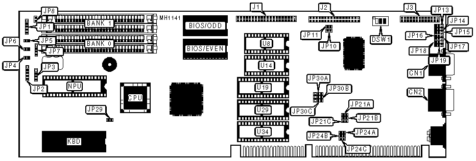
INTERLOGIC INDUSTRIES
SBC6126
|
Processor |
80286 |
|
Processor Speed |
16MHz |
|
Chip Set |
Headland |
|
Max. Onboard DRAM |
4MB |
|
Cache |
None |
|
BIOS |
AMI |
|
Dimensions |
350mm x 121mm |
|
I/O Options |
Floppy drive interface, IDE interface, parallel port, serial ports (2) |
|
NPU Options |
80287 |

|
CONNECTIONS |
|||
|
Purpose |
Location |
Purpose |
Location |
|
Serial port 1 |
CN1 |
Speaker |
JP3 |
|
Serial port 2 |
CN2 |
Reset switch |
JP4 |
|
IDE interface |
J1 |
Turbo LED |
JP5 |
|
Floppy drive interface |
J2 |
Turbo switch |
JP6 |
|
Parallel port |
J3 |
External battery |
JP7 |
|
Auxiliary keyboard |
JP1 |
IDE interface LED |
JP8 |
|
Power LED & keylock |
JP2 |
|
|
|
USER CONFIGURABLE SETTINGS |
|||
|
Function |
Jumper |
Position |
|
|
» |
IDE interface enabled |
JP10 & JP11 |
Closed |
|
|
IDE interface disabled |
JP10 & JP11 |
Open |
|
» |
Factory configured - do not alter |
JP13 |
pins 1 & 2 closed |
|
» |
Floppy drive interface enabled |
JP14 |
pins 1 & 2 closed |
|
|
Floppy drive interface disabled |
JP14 |
pins 2 & 3 closed |
|
» |
Monitor type select color |
JP29 |
Closed |
|
|
Monitor type select monochrome |
JP29 |
Open |
|
SERIAL PORT CONFIGURATION |
||||
|
Serial Port 1 (CN1) |
Serial Port 2 (CN2) |
JP15 |
JP16 |
JP17 |
|
COM1 |
COM2 |
pins 1 & 2 |
pins 1 & 2 |
pins 1 & 2 |
|
COM1 |
Disabled |
pins 1 & 2 |
pins 2 & 3 |
pins 1 & 2 |
|
COM2 |
COM1 |
pins 2 & 3 |
pins 1 & 2 |
pins 1 & 2 |
|
Disabled |
COM1 |
pins 2 & 3 |
pins 1 & 2 |
pins 2 & 3 |
|
Disabled |
COM2 |
pins 1 & 2 |
pins 1 & 2 |
pins 2 & 3 |
|
COM2 |
Disabled |
pins 2 & 3 |
pins 2 & 3 |
pins 1 & 2 |
|
Disabled |
Disabled |
pins 1 & 2 |
pins 2 & 3 |
pins 2 & 3 |
|
Note: Pins designated should be in the closed position. |
||||
|
PARALLEL PORT CONFIGURATION |
||
|
Parallel Port |
JP18 |
JP19 |
|
LPT1 |
pins 1 & 2 closed |
pins 2 & 3 closed |
|
LPT2 |
pins 1 & 2 closed |
pins 1 & 2 closed |
|
LPT3 |
pins 2 & 3 closed |
pins 1 & 2 closed |
|
Disabled |
pins 2 & 3 closed |
pins 2 & 3 closed |
|
WATCHDOG TIMER CONFIGURATION |
|||
|
Timer Mode |
JP21A |
JP21B |
JP21C |
|
Always enabled |
closed |
open |
open |
|
Software selectable 1 |
open |
closed |
open |
|
Always disabled |
open |
open |
closed |
|
Note 1 :To enable and refresh the timer, read I/O port 443h. To disable the timer, read I/O port 043h. |
|||
|
WATCHDOG TIMER INTERVAL CONFIGURATION |
|||
|
Timer Interval |
JP24A |
JP24B |
JP24C |
|
Short (1.5 seconds) |
closed |
open |
open |
|
Medium (15 seconds) |
open |
closed |
open |
|
Long (150 seconds) |
open |
open |
closed |
|
Note: When the Watchdog Timer is enabled, it will reboot the system at the above selected interval unless I/O port 443h is read before the timer expires. The timer is only accurate ± 30% - so if the timer is set to reboot the system every 15 seconds, make sure I/O port 443h is read within approximately every 10 seconds. |
|||
|
ROM DISK CONFIGURATION |
||||
|
EPROM Size |
Drive Emulation |
JP30A |
JP30B |
JP30C |
|
1M (360KB floppy) |
A: |
pins 1 & 2 closed |
pins 1 & 2 closed |
pins 1 & 2 closed |
|
1M (360KB floppy) |
B: |
pins 1 & 2 closed |
pins 1 & 2 closed |
pins 2 & 3 closed |
|
4M (1.44MB floppy) |
A: |
pins 2 & 3 closed |
pins 2 & 3 closed |
pins 1 & 2 closed |
|
4M (1.44MB floppy) |
B: |
pins 2 & 3 closed |
pins 2 & 3 closed |
pins 2 & 3 closed |
|
Note: The utility "COOKROM.EXE" will convert either a 360KB or a 1.44MB floppy disk into three files: ROM1.BIN, ROM2.BIN and ROM3.BIN (If the disk doesn't contain much data, then there may be only one or two files created). These files then may be placed (using an EPROM Burner that supports an Intel D27C0040 512K x 8 EPROM) onto up to three EPROMs. The EPROM that now contains the file ROM1.BIN should be placed in socket U19. The EPROM that now contains the file ROM2.BIN should be placed in socket U29. The EPROM that now contains the file ROM3.BIN should be placed in socket U34. |
||||
|
ROM DISK BIOS SEGMENT ADDRESS |
||||
|
ROM Disk Address |
DSW1/switch 1 |
DSW1/switch 2 |
DSW1/switch 3 |
|
|
|
Disabled |
closed |
closed |
closed |
|
|
C400h |
closed |
closed |
open |
|
|
C800h |
closed |
open |
closed |
|
|
CC00h |
closed |
open |
open |
|
» |
D000h |
open |
closed |
closed |
|
|
D400h |
open |
closed |
open |
|
|
D800h |
open |
open |
closed |
|
|
DC00h |
open |
open |
open |
|
Note: The ROM disk BIOS populates socket U14. |
||||
|
DRAM CONFIGURATION |
||
|
Size |
Bank 0 |
Bank 1 |
|
512KB |
(2) 256K x 9 |
NONE |
|
1MB |
(2) 256K x 9 |
(2) 256K x 9 |
|
2MB |
(2) 1M x 9 |
NONE |
|
4MB |
(2) 1M x 9 |
(2) 1M x 9 |