DD & TT ENTERPRISE USA COMPANY
DT ESCORT SYSTEM BOARD A
|
Processor |
80386SX/80486SLC |
|
Processor Speed |
25/33/40MHz |
|
Chip Set |
Symphony |
|
Max. Onboard DRAM |
16MB |
|
Cache |
None |
|
BIOS |
AMI |
|
Dimensions |
330mm x 218mm |
|
I/O Options |
Floppy drive interface, IDE interface, parallel port Proprietary EISA riser card slot, PS/2 mouse port Serial port (2), VGA port, video feature connector |
|
NPU Options |
80387SX/CX487SLC |
|
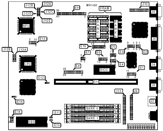
CONNECTIONS |
|||
|
Purpose |
Location |
Purpose |
Location |
|
PS/2 mouse port |
J2 |
Reset switch |
J12A |
|
Serial port (COM 1) |
J3 |
Turbo switch |
J12B |
|
Serial port (COM 2) |
J4 |
Turbo LED |
J12C |
|
Parallel port |
J5 |
IDE interface LED |
J12D |
|
VGA port |
J6 |
Not used |
J12E |
|
Floppy drive interface |
J9 |
Speaker |
J13A |
|
Video feature port |
J10 |
Power LED & keylock |
J13B |
|
IDE interface |
J11 |
Proprietary riser card slot |
S1 |
|
USER CONFIGURABLE SETTINGS |
|||
|
Function |
Jumper |
Position |
|
|
» |
Floppy drive disabled |
E1 |
pins 1 & 3 closed |
|
|
Floppy drive enabled |
E1 |
pins 3 & 5 closed |
|
|
Floppy drive address select 3FO-3F7 |
E1 |
pins 7 & 9 closed |
|
|
Floppy drive address select 370-377 |
E1 |
pins 9 & 11 closed |
|
» |
IDE interface disabled |
E1 |
pins 2 & 4 closed |
|
|
IDE interface enabled |
E1 |
pins 4 & 6 closed |
|
|
IDE interface address 3FO-3F7, 1FO-1F7 |
E1 |
pins 8 & 10 closed |
|
|
IDE interface address 370-377, 170-177 |
E1 |
pins 20 & 12 closed |
|
» |
On board video enabled |
E2 |
pins 1 & 2, 3 & 4, 5 & 6 closed |
|
|
On board video disabled |
E2 |
pins 1 & 2, 3 & 4, 5 & 6 open |
|
» |
BIOS device select 1MB |
E6 |
pins 1 & 2 closed |
|
|
BIOS device select 2MB |
E6 |
pins 3 & 5 closed |
|
|
BIOS device select read only |
E6 |
pins 2 & 4, 7 & 9, 8 & 10 closed |
|
» |
BIOS device select read/write |
E6 |
pins 4 & 6, 9 & 11, 10 & 12 |
|
» |
Chipset mode select 2x for 40MHz or less |
E7 |
pins 3 & 5 closed |
|
|
Chipset mode select 1x for true 50MHz only |
E7 |
pins 1 & 3 closed |
|
|
Chipset mode RDY1 set for 1X mode |
E7 |
pins 4 & 6 closed |
|
|
Chipset mode RDY2 set for 2X mode |
E7 |
pins 2 & 4 closed |
|
» |
Chipset mode burst rate select 3-2-2-2 |
E8 |
pins 23 & 24 closed |
|
|
Chipset mode burst rate select 2-1-1-1 |
E8 |
pins 23 & 24 open |
|
» |
Chipset mode write select 0 wait state |
E8 |
pins 25 & 26 closed |
|
|
Chipset mode write select 1 wait state |
E8 |
pins 25 & 26 open |
|
» |
PS/2 mouse enable at IRQ12 |
E10 |
Closed |
|
|
PS/2 mouse disable |
E10 |
Open |
|
» |
CMOS memory normal |
E11 |
Open |
|
|
CMOS memory clear |
E11 |
Closed |
|
» |
CPU speed select iOSC/2 |
E12 |
pins 2 & 3 closed |
|
|
CPU speed select iOSC/1 |
E12 |
pins 1 & 2 closed |
|
» |
Factory configured - do not alter |
E15 |
pins 1 & 2 closed |
|
» |
Factory configured - do not alter |
E16/1, 3 & 5 |
pins 3 & 5 closed |
|
» |
Factory configured - do not alter |
E16/2, 4, & 6 |
pins 4 & 6 closed |
|
» |
Factory configured - do not alter |
E16/7, 9 & 11 |
pins 9 & 11 closed |
|
» |
Factory configured - do not alter |
E16/7 & 8 |
Closed |
|
» |
Factory configured - do not alter |
E16/8 & 10 |
N/A |
|
» |
Factory configured - do not alter |
E16/11 & 12 |
Open |
|
USER CONFIGURABLE SETTINGS (CONTINUED) |
|||
|
Function |
Jumper |
Position |
|
|
» |
Factory configured - do not alter |
E16/13 & 14 |
Closed |
|
» |
Factory configured - do not alter |
E16/15 & 16 |
Closed |
|
» |
Factory configured - do not alter |
E16/17 & 18 |
Closed |
|
Note: If there is no monochrome Hercules card present then the system will automatically assume that address 378h is LPT1 and address 278h is LPT2. Pins designated should be in the closed position. |
|||
|
DRAM CONFIGURATION |
||
|
Size |
Bank 0 |
Bank 1 |
|
512KB |
(2) 256K x 9 |
NONE |
|
1MB |
(2) 256K x 9 |
(2) 256K x 9 |
|
2MB |
(2) 1M x 9 |
NONE |
|
2.5MB |
(2) 256K x 9 |
(2) 1M x 9 |
|
4MB |
(2) 1M x 9 |
(2) 1M x 9 |
|
8MB |
(2) 4M x 9 |
NONE |
|
8.5MB |
(2) 256K x 9 |
(2) 4M x 9 |
|
10MB |
(2) 1M x 9 |
(2) 4M x 9 |
|
16MB |
(2) 4M x 9 |
(2) 4M x 9 |
|
16MB |
(2) 16M x 9 |
(2) 16M x 9 |
|
CPU SPEED CONFIGURATION |
|||
|
Speed |
E14/pins 1 & 2 |
E14/pins 3 & 4 |
E14/pins 5 & 6 |
|
25MHz |
Open |
Closed |
Closed |
|
33MHz |
Open |
Closed |
Open |
|
40MHz |
Open |
Open |
Closed |
|
25MHz |
Open |
Closed |
Closed |
|
33MHz |
Open |
Closed |
Open |
|
SERIAL PORT A (J3) CONFIGURATION |
|||
|
COM |
I/O Address |
E5 |
|
|
» |
COM1 |
3F8h |
pins 3 & 5, 2 & 4, 7 & 8 |
|
|
COM3 |
3E8h |
pins 1 & 3, 4 & 6, 7 & 8 |
|
|
COM4 |
2E8h |
pins 3 & 5, 4 & 6, 7 & 8 |
|
|
Disabled |
N/A |
pins 1 & 3, 2 & 4 |
|
Note: pins designated should be in the closed position. |
|||
|
SERIAL PORT B (J4) CONFIGURATION |
|||
|
COM |
I/O Address |
E4 |
|
|
» |
COM2 |
2F8h |
pins 3 & 5, 2 & 4, 7 & 8 |
|
|
COM3 |
3E8h |
pins 3 & 5, 4 & 6, 7 & 8 |
|
|
COM4 |
2E8h |
pins 1 & 3, 4 & 6, 7 & 8 |
|
|
Disabled |
N/A |
pins 1 & 3, 2 & 4 |
|
Note:pins designated should be in the closed position. |
|||
|
PARALLEL PORT (J5) CONFIGURATION |
||||
|
COM |
IRQ |
I/O Address |
E3 |
|
|
» |
LPT1 |
IRQ7 |
3BCh |
pins 3 & 5, 4 & 6, 7 & 8 |
|
|
LPT1 |
IRQ5 |
3BCh |
pins 3 & 5, 4 & 6, 9 & 10 |
|
|
LPT2 |
IRQ7 |
378h |
pins 3 & 5, 2 & 6, 7 & 8 |
|
|
LPT2 |
IRQ5 |
378h |
pins 3 & 5, 2 & 6, 9 & 10 |
|
|
LPT3 |
IRQ7 |
278h |
pins 1 & 3, 4 & 6, 7 & 8 |
|
|
LPT3 |
IRQ5 |
278h |
pins 1 & 3, 4 & 6, 9 & 10 |
|
|
Disabled |
N/A |
N/A |
pins 1 & 3, 2 & 4 |
|
Note: pins designated should be in the closed position. |
||||
|
VIDEO MEMORY CONFIGURATION |
||
|
Size |
Bank 0 |
Bank 1 |
|
512KB |
(4) 44256 |
NONE |
|
1024KB |
(4) 44256 |
(4) 44256 |
|
Note: Bank 0 is permanently soldered onto the board. |
||