QUATECH, INC.
DM8-10
|
Category |
Digital to analog signal converter |
|
Chipset Controller |
Unidentified |
|
I /O Options Supported |
Digital signal input via module connector |
|
Maximum Onboard Memory |
N/A |
|
CONNECTIONS | |||
|
Purpose |
Location |
Purpose |
Location |
|
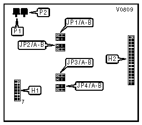
Output connector |
H1 |
Potentiometer: ref. voltage adjust ch. 4-7 |
P1 |
|
Expansion card connector |
H2 |
Potentiometer: ref. voltage adjust ch. 0-3 |
P2 |
|
CHANNEL 0 OUTPUT SIGNAL | ||
|
» Setting |
JP1/jumper A | |
| » |
Bipolar/-5 to 5V |
Pins 2 & 3 closed |
| » |
Unipolar/0 to 5V |
Pins 1 & 2 closed |
|
CHANNEL 1 OUTPUT SIGNAL | ||
|
» Setting |
JP1/jumper B | |
| » |
Bipolar/-5 to 5V |
Pins 2 & 3 closed |
| » |
Unipolar/0 to 5V |
Pins 1 & 2 closed |
|
CHANNEL 2 OUTPUT SIGNAL | ||
|
» Setting |
JP2/jumper A | |
| » |
Bipolar/-5 to 5V |
Pins 2 & 3 closed |
| » |
Unipolar/0 to 5V |
Pins 1 & 2 closed |
|
CHANNEL 3 OUTPUT SIGNAL | ||
|
» Setting |
JP2/jumper B | |
| » |
Bipolar/-5 to 5V |
Pins 2 & 3 closed |
| » |
Unipolar/0 to 5V |
Pins 1 & 2 closed |
|
CHANNEL 4 OUTPUT SIGNAL | ||
|
» Setting |
JP3/jumper A | |
| » |
Bipolar/-5 to 5V |
Pins 2 & 3 closed |
| » |
Unipolar/0 to 5V |
Pins 1 & 2 closed |
|
CHANNEL 5 OUTPUT SIGNAL | ||
|
» Setting |
JP3/jumper B | |
| » |
Bipolar/-5 to 5V |
Pins 2 & 3 closed |
| » |
Unipolar/0 to 5V |
Pins 1 & 2 closed |
|
CHANNEL 6 OUTPUT SIGNAL | ||
|
» Setting |
JP4/jumper A | |
| » |
Bipolar/-5 to 5V |
Pins 2 & 3 closed |
| » |
Unipolar/0 to 5V |
Pins 1 & 2 closed |
|
CHANNEL 7 OUTPUT SIGNAL | ||
|
» Setting |
JP4/jumper B | |
| » |
Bipolar/-5 to 5V |
Pins 2 & 3 closed |
| » |
Unipolar/0 to 5V |
Pins 1 & 2 closed |
|
MISCELLANEOUS TECHNICAL NOTES |
|
The DM8-10 is a modular daughter-card designed to work with the Quatech PXB-721 or MXI-241. Channel 0 through channel 6 output is taken from pins 1 to 7, respectively, of header H1 while channel 7 output is taken from pin 11 of header H1, 2, or 3 of header H1. The rest of the pins of header H1 are grounded. |