AMERICAN DATA AQUISITION CORPORATION
5508LC REV. 1-USI=1
|
Card Type |
Data Aquisition |
|
Chip Set |
Unidentified |
|
Maximum Onboard Memory |
Unidentified |
|
I/O Options |
Analog input, digital input |
|
Hard Drives supported |
None |
|
Floppy drives supported |
None |
|
Data Bus |
8-bit ISA |
|
Card Size |
Half length |
|
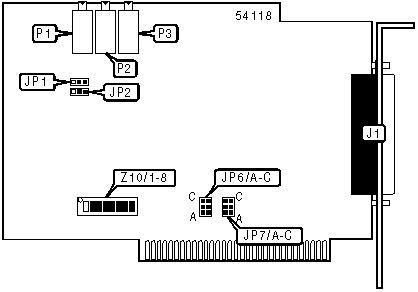
CONNECTIONS | |||
|
Function |
Label |
Function |
Label |
|
37-pin analog/digital signals connector |
J1 |
A/D converter range selector |
P2 |
|
Bipolar & offset selector |
P1 |
Unipolar zero selector |
P3 |
|
USER CONFIGURABLE SETTINGS | |||
|
Function |
Label |
Position | |
| » |
Factory configured - do not alter |
Z10/7 |
Off |
|
GAIN SELECTION | |||
|
Function |
W1 |
W2 | |
| » |
Programmable gain options: x1, x2, x5, x10 |
Open |
Open |
|
Programmable gain options: x1, x2, x4, x8 |
Closed |
Closed | |
|
DMA CHANNEL SELECTION | |||||||
|
Channel |
JP6/A |
JP6/B |
JP6/C |
JP7/A |
JP7/B |
JP7/C | |
| » |
Disabled |
Open |
Open |
Open |
Open |
Open |
Open |
|
1 |
Closed |
Open |
Open |
Closed |
Open |
Open | |
|
2 |
Open |
Closed |
Open |
Open |
Closed |
Open | |
|
3 |
Open |
Open |
Closed |
Open |
Open |
Closed | |
|
A/D RANGE SELECTION | |||||
|
Polarity |
Voltage |
JP1 |
JP2 |
Z10/8 | |
| » |
Bipolar |
+ 5V |
Pins 2 & 3 closed |
Pins 1 & 2 closed |
On |
|
Unipolar |
+0-10V |
Pins 1 & 2 closed |
Pins 1 & 2 closed |
Off | |
|
Bipolar |
+ 10V |
Pins 2 & 3 closed |
Pins 2 & 3 closed |
On | |
|
BASE I/O ADDRESS SELECTION | |||||||
|
Setting |
Z10/1 |
Z10/2 |
Z10/3 |
Z10/4 |
Z10/5 |
Z10/6 | |
|
000h |
Off |
Off |
Off |
Off |
Off |
Off | |
|
010h |
Off |
Off |
Off |
Off |
Off |
On | |
|
020h |
Off |
Off |
Off |
Off |
On |
Off | |
|
030h |
Off |
Off |
Off |
Off |
On |
On | |
|
040h |
Off |
Off |
Off |
On |
Off |
Off | |
| » |
120h |
Off |
On |
Off |
Off |
On |
Off |
|
3B0h |
On |
On |
On |
Off |
On |
On | |
|
3C0h |
On |
On |
On |
On |
Off |
Off | |
|
3D0h |
On |
On |
On |
On |
Off |
On | |
|
3E0h |
On |
On |
On |
On |
On |
Off | |
|
3F0h |
On |
On |
On |
On |
On |
On | |
|
Note: A total of 64 base address settings are available. The switches are a binary representation of the decimal memory addresses. Z10/1 is the Most Significant Bit and switch Z10/6 is the Least Significant Bit. The switches have the following decimal values: Z10/1=512, Z10/2=256, Z10/3=128, Z10/4=64, Z10/5=32, Z10/6=16. Turn off the switches and add the values of the switches to obtain the correct memory address. (On=1, Off=0) | |||||||
|
MISCELLANEOUS TECHNICAL NOTES |
|
Exact location of jumpers W1 & W2 is unidentified. |