UNIDENTIFIED
P55-ET
|
Processor |
Pentium |
|
Processor Speed |
75/90/100/120/133/150/166MHz |
|
Chip Set |
Intel |
|
Video Chip Set |
None |
|
Maximum Onboard Memory |
128MB (EDO supported) |
|
Maximum Video Memory |
None |
|
Cache |
256/512KB |
|
BIOS |
Award |
|
Dimensions |
330mm x 218mm |
|
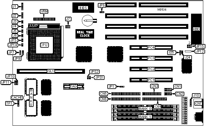
I/O Options |
32-bit PCI slots (4), floppy drive interface, green PC connector, IDE interfaces (2), parallel port, PS/2 mouse port, PS/2 mouse interface, serial ports (2), cache slot, VRM connector |
|
NPU Options |
None |
|
CONNECTIONS | |||
|
Purpose |
Location |
Purpose |
Location |
|
Serial port 2 |
CN1 |
Turbo switch |
J4 |
|
Serial port 1 |
CN2 |
Turbo LED |
J5 |
|
Parallel port |
CN3 |
Green PC LED |
J6 |
|
Floppy drive interface |
CN4 |
Chassis fan power |
J7 |
|
IDE interface 2 |
CN5 |
PS/2 mouse interface |
J10 |
|
IDE interface 1 |
CN6 |
IDE interface LED |
JP5 |
|
PS/2 mouse port |
CN7 |
Green PC connector |
JP14 |
|
Power LED & keylock |
J1 |
32-bit PCI slots |
PC1 - PC4 |
|
Speaker |
J2 |
Cache slot |
SL1 |
|
Reset switch |
J3 |
VRM connector |
VRM |
|
USER CONFIGURABLE SETTINGS | |||
|
Function |
Label |
Position | |
|
» |
SMC chip enabled |
J24 |
Open |
|
SMC chip disabled |
J24 |
Closed | |
|
» |
Flash BIOS voltage select 5v |
JP6 |
Pins 1 & 2 closed |
|
Flash BIOS voltage select 12v |
JP6 |
Pins 2 & 3 closed | |
|
Jumper information unavailable |
JP12 |
Unidentified | |
|
» |
Clock rate set as AT CLOCK |
JP15 |
Pins 1 & 2 closed |
|
Clock rate set as 12MHz |
JP15 |
Pins 2 & 3 closed | |
|
DRAM CONFIGURATION | ||
|
Size |
Bank 0 |
Bank 1 |
|
8MB |
(2) 1M x 36 |
None |
|
16MB |
(2) 1M x 36 |
(2) 1M x 36 |
|
16MB |
(2) 2M x 36 |
None |
|
24MB |
(2) 1M x 36 |
(2) 2M x 36 |
|
24MB |
(2) 2M x 36 |
(2) 1M x 36 |
|
32MB |
(2) 2M x 36 |
(2) 2M x 36 |
|
32MB |
(2) 4M x 36 |
None |
|
40MB |
(2) 1M x 36 |
(2) 4M x 36 |
|
40MB |
(2) 4M x 36 |
(2) 1M x 36 |
|
48MB |
(2) 2M x 36 |
(2) 4M x 36 |
|
48MB |
(2) 4M x 36 |
(2) 2M x 36 |
|
64MB |
(2) 4M x 36 |
(2) 4M x 36 |
|
64MB |
(2) 8M x 36 |
None |
|
72MB |
(2) 1M x 36 |
(2) 8M x 36 |
|
72MB |
(2) 8M x 36 |
(2) 1M x 36 |
|
80MB |
(2) 2M x 36 |
(2) 8M x 36 |
|
80MB |
(2) 8M x 36 |
(2) 2M x 36 |
|
96MB |
(2) 4M x 36 |
(2) 8M x 36 |
|
96MB |
(2) 8M x 36 |
(2) 4M x 36 |
|
128MB |
(2) 8M x 36 |
(2) 8M x 36 |
|
Note: Board accepts EDO memory. Board also accepts x 32 SIMMs. | ||
|
CACHE CONFIGURATION | |||
|
Size |
Bank 0 |
TAG |
SL1 |
|
256KB (A) |
(2) 32K x 32 |
None |
256KB module installed |
|
256KB (B) |
(2) 32K x 32 |
(1) 8K/16K x 8 |
Not installed |
|
512KB (A) |
(2) 64K x 32 |
(1) 16K/32K x 8 |
Not installed |
|
512KB (B) |
(2) 32K x 32 |
(1) 16K/32K x 8 |
256KB module installed |
|
Note: If 256KB (A) configuration is used, see jumper setting for TP1 below. | |||
|
CACHE JUMPER CONFIGURATION | ||
|
Size |
JP10 |
JP11 |
|
256KB (B) |
Pins 1 & 2 closed |
Pins 1 & 2 closed |
|
512KB (A) |
Pins 1 & 2 closed |
Pins 1 & 2 closed |
|
512KB (B) |
Pins 2 & 3 closed |
Pins 2 & 3 closed |
|
CACHE JUMPER CONFIGURATION | |
|
Size |
TP1 |
|
Bank 0 enabled |
Open |
|
Bank 0 disabled |
Pins 1 & 2, 3 & 4 closed |
|
CPU SPEED SELECTION | |||||||
|
CPU speed |
Clock speed |
Multiplier |
J25 |
JP7 |
JP9 |
JPS1 |
JPS2 |
|
75MHz |
50MHz |
1.5x |
1 & 2 |
2 & 3 |
2 & 3 |
Open |
Open |
|
90MHz |
60MHz |
1.5x |
2 & 3 |
2 & 3 |
2 & 3 |
Closed |
Open |
|
100MHz |
66MHz |
1.5x |
2 & 3 |
2 & 3 |
2 & 3 |
Closed |
Closed |
|
120MHz |
60MHz |
2x |
2 & 3 |
1 & 2 |
2 & 3 |
Closed |
Open |
|
133MHz |
66MHz |
2x |
2 & 3 |
1 & 2 |
2 & 3 |
Closed |
Closed |
|
150MHz |
60MHz |
2.5x |
2 & 3 |
1 & 2 |
1 & 2 |
Closed |
Open |
|
166MHz |
66MHz |
2.5x |
2 & 3 |
1 & 2 |
1 & 2 |
Closed |
Closed |
|
Note: Pins designated should be in the closed position. | |||||||
|
CPU TYPE SELECTION | |
|
Type |
JP1 |
|
P54C/P54CS |
Pins 1 & 2 closed |
|
P55C/P55CT |
Pins 2 & 3 closed |
|
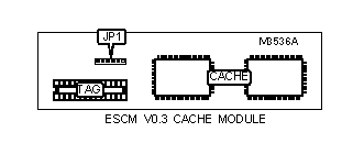
CACHE JUMPER CONFIGURATION (ESCM CACHE MODULE) | |
|
Size |
JP1 |
|
256KB |
Pins 1 & 2, 5 & 6 closed |
|
512KB |
Pins 2 & 3, 4 & 5 closed |