IPC CORPORATION, LTD.
IPC MBFDSIIS-25
|
Processor |
80386SX (exact location unidentified) |
|
Processor Speed |
25MHz |
|
Chip Set |
Unidentified |
|
Maximum Onboard Memory |
16MB |
|
Cache |
512KB |
|
BIOS |
Unidentified |
|
Dimensions |
330mm x 218mm |
|
I/O Options |
External memory card, floppy drive interface, hard drive interface, parallel ports (2), serial ports (4), VGA port, cache connector, drawer port connector, magnetic card reader connector, touch screen board connector, riser slot |
|
NPU Options |
Unidentified |
|
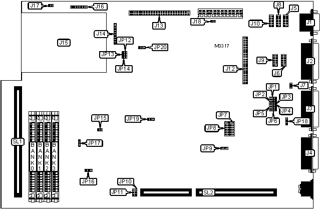
CONNECTIONS | |||
|
Function |
Label |
Function |
Label |
|
VGA port |
J1 |
Drawer port connector |
J10 |
|
Parallel port 2 |
J2 |
Hard drive interface |
J12 |
|
Parallel port 1 |
J3 |
Touch screen board connector |
J13 |
|
Floppy drive interface |
J4 |
Magnetic card reader connector |
J14 |
|
Serial port 1 |
J5 |
Cache connector |
J15 |
|
Serial port 2 |
J6 |
Multi-level keylock |
J16 |
|
Chassis fan power (not used) |
J7 |
Chassis fan power |
J17 |
|
Serial port 3 |
J8 |
External memory card |
SL1 |
|
Serial port 4 |
J9 |
Riser slot |
SL2 |
|
USER CONFIGURABLE SETTINGS | |||
|
Setting |
Label |
Position | |
|
» |
Factory configured - do not alter |
J18 |
N/A |
|
» |
Multi I/O address & data register address select 398H/399H |
JP1 |
Pins 2 & 3 closed |
|
Multi I/O address & data register address 26EH/26FH |
JP1 |
Pins 1 & 2 closed | |
|
» |
Multi I/O configuration registers |
JP2 |
Pins 1 & 2 closed |
|
» |
Multi I/O configuration registers |
JP3 |
Pins 2 & 3 closed |
|
» |
Multi I/O configuration registers |
JP4 |
Pins 2 & 3 closed |
|
» |
Multi I/O configuration registers |
JP5 |
Pins 2 & 3 closed |
|
» |
Multi I/O configuration registers |
JP6 |
Pins 2 & 3 closed |
|
» |
CMOS memory normal operation (1287A) |
JP9 |
Open |
|
CMOS memory clear (1287A) |
JP9 |
Pins 1 & 2 closed | |
|
» |
CMOS memory normal operation (1287) |
JP9 |
Open |
|
CMOS memory clear (1287) |
JP9 |
Pins 2 & 3 closed | |
|
» |
Cache window address select DC000H - DFFFFH |
JP12 |
Open |
|
Cache window address select ECOOOH - EFFFFH |
JP12 |
Closed | |
|
Reset disabled |
JP15 |
Open | |
|
Reset enabled |
JP15 |
Closed | |
|
» |
AT bus speed select 8MHz |
JP16 |
Pins 1 & 2 closed |
|
AT bus speed select 12MHz |
JP16 |
Pins 2 & 3 closed | |
|
» |
Factory configured - do not alter |
JP18 |
Pins 2 & 3 closed |
|
» |
LCD contrast select LCDENA# signal for LCD power sequencing |
JP19 |
Pins 2 & 3 closed |
|
LCD contrast select PWROFF signal for power sequencing |
JP19 |
Pins 1 & 2 closed | |
|
Touch screen select resistive keys |
JP20 |
Pins 1 & 2 closed | |
|
Touch screen select capacitive touch screen |
JP20 |
Pins 2 & 3 closed | |
|
DRAM | |||||
|
Size |
Bank 0 |
Bank 1 |
Bank 2 |
Bank 3 |
SL1 |
|
1MB |
(1) 256K x 9 |
(1) 256K x 9 |
(1) 256K x 9 |
(1) 256K x 9 |
None |
|
2MB |
(1) 1M x 9 |
(1) 1M x 9 |
None |
None |
None |
|
2MB |
(1) 256K x 9 |
(1) 256K x 9 |
(1) 256K x 9 |
(1) 256K x 9 |
1MB on card |
|
4MB |
(1) 1M x 9 |
(1) 1M x 9 |
(1) 1M x 9 |
(1) 1M x 9 |
None |
|
8MB |
(1) 1M x 9 |
(1) 1M x 9 |
(1) 1M x 9 |
(1) 1M x 9 |
4MB on card |
|
8MB |
(1) 4M x 9 |
(1) 4M x 9 |
None |
None |
None |
|
16MB |
(1) 4M x 9 |
(1) 4M x 9 |
(1) 4M x 9 |
(1) 4M x 9 |
None |
|
CACHE SIZE |
|
Note: 512KB cache card is installed at J15. |
|
CACHE WAIT STATE | |||
|
Setting |
JP13 |
JP14 | |
| » |
0 wait state |
Closed |
Open |
|
1 wait states |
Open |
Closed | |
|
CPU PIPELINE | ||||
|
Setting |
JP10 |
JP11 |
JP17 | |
| » |
Pipeline enabled |
Pins 1 & 2 closed |
Pins 2 & 3 closed |
Pins 2 & 3 closed |
|
Pipeline disabled |
Pins 2 & 3 closed |
Pins 1 & 2 closed |
Pins 1 & 2 closed | |
|
PARALLEL PORT 2 IRQ | ||
|
IRQ |
JP7 | |
| » |
IRQ5 |
Pins 1 & 2 closed |
|
IRQ7 |
Pins 3 & 4 closed | |
|
SERIAL PORT 3 IRQ | |||
|
Setting |
IRQ |
JP7 | |
| » |
COM3 |
IRQ11 |
Pins 9 & 10 closed |
|
COM3 |
IRQ4 |
Pins 11 & 12 closed | |
|
SERIAL PORT 4 IRQ | |||
|
Setting |
IRQ |
JP7 | |
| » |
COM4 |
IRQ10 |
Pins 5 & 6 closed |
|
COM4 |
IRQ3 |
Pins 7 & 8 closed | |
|
PARALLEL PORT 2 ADDRESS | |||
|
Setting |
Address |
JP8 | |
| » |
LPT2 |
278H - 27FH |
Pins 9 & 10 closed |
|
LPT1 |
378H - 37FH |
Pins 11 & 12 closed | |
|
SERIAL PORT 3 ADDRESS | |||
|
Setting |
Address |
JP8 | |
|
COM1 |
3F8H - 3FFH |
Pins 3 & 4 closed | |
| » |
COM3 |
3E8H - 3EFH |
Pins 1 & 2 closed |
|
SERIAL PORT 4 ADDRESS | |||
|
Setting |
Address |
JP8 | |
|
COM2 |
2F8H - 2FFH |
Pins 7 & 8 closed | |
| » |
COM4 |
2E8H - 2EFH |
Pins 5 & 6 closed |