LEADING EDGE PRODUCTS, INC.
MODEL D (REVISION 1 & 5)
|
Processor |
8088 (Exact location unknown.) |
|
Processor Speed |
4.77MHz |
|
Chip Set |
Unknown |
|
Max. Onboard DRAM |
640KB |
|
Cache |
None |
|
BIOS |
Unknown |
|
Dimensions |
254mm x 218mm |
|
I/O Options |
Color monitor port, floppy drive interface, light pen connector, monochrome monitor port, parallel port, serial port |
|
NPU Options |
8087 (Exact location unknown.) |
|
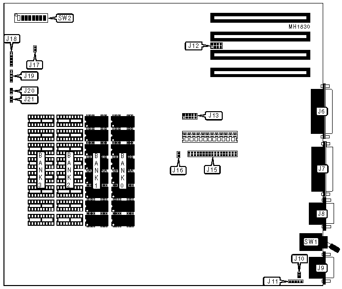
CONNECTIONS | |||
|
Purpose |
Location |
Purpose |
Location |
|
Parallel port |
J6 |
Floppy drive interface |
J15 |
|
Serial port |
J7 |
Keyboard |
J18 |
|
Color monitor port |
J8 |
Speaker |
J19 |
|
Monochrome port |
J9 |
Reset switch |
J20 |
|
Light pen connector |
J11 |
Power-on LED indicator |
J21 |
|
USER CONFIGURABLE SETTINGS | |||
|
Function |
Jumper |
Position | |
|
» |
Factory configured - do not alter |
J5 |
N/A |
|
» |
Monitor enabled |
J10 |
Closed |
|
Monitor disabled |
J10 |
Open | |
|
» |
Floppy drive interface enabled |
J13 |
pins 4 & 9 closed |
|
Floppy drive interface disabled |
J13 |
pins 4 & 9 open | |
|
» |
Serial port enabled |
J13 |
pins 5 & 10 closed |
|
Serial port disabled |
J13 |
pins 5 & 10 open | |
|
» |
Parallel port enabled |
J13 |
pins 3 & 8 closed |
|
Parallel port disabled |
J13 |
pins 3 & 8 open | |
|
» |
Real Time Clock enabled |
J13 |
pins 2 & 7 closed |
|
Real Time Clock disabled |
J13 |
pins 2 & 7 open | |
|
» |
Factory configured - do not alter |
J13 |
pins 1 & 6 open |
|
» |
BIOS ROM type 8/16K |
J16 |
Open |
|
BIOS ROM type 32K |
J16 |
Closed | |
|
» |
Video mode TTL mononchrome |
SW1 |
Up |
|
Video mode CGA |
SW1 |
Down | |
|
» |
Factory configured - do not alter |
SW2/Switch 1 |
Off |
|
» |
NPU disabled |
SW2/Switch 2 |
On |
|
NPU enabled |
SW2/Switch 2 |
Off | |
|
» |
Factory configured - do not alter |
SW2/Switch 3 |
On |
|
» |
Memory test 64KB |
SW2/Switch 4 |
On |
|
Memory test all |
SW2/Switch 4 |
Off | |
|
» |
Factory configured - do not alter |
SW2/Switch 5 |
Off |
|
» |
Factory configured - do not alter |
SW2/Switch 6 |
Off |
|
Note:The exact location of J5 is unknown. | |||
|
DRAM CONFIGURATION | |||||
|
Size |
Bank 0 |
Bank 1 |
Bank 2 |
Bank 3 |
J17 |
|
256KB |
(9) 4164 |
(9) 4164 |
(9) 4164 |
(9) 4164 |
Closed |
|
640KB |
(9) 4164 |
(9) 4164 |
(9) 41256 |
(9) 41256 |
Open |
|
FLOPPY DISK DRIVES INSTALLED | ||
|
Number of Drives |
SW2/Switch 7 |
SW2/Switch 8 |
|
1 |
On |
On |
|
2 |
Off |
On |
|
3 |
On |
Off |
|
4 |
Off |
Off |
|
REAL TIME CLOCK INTERRUPT SELECT | |
|
IRQ |
J12 |
|
2 |
pins 1 & 5 closed |
|
4 |
pins 2 & 6 closed |
|
5 |
pins 3 & 7 closed |
|
7 |
pins 4 & 8 closed |