ELITEGROUP COMPUTER SYSTEMS, INC.
TS54P AIO (V1.4)
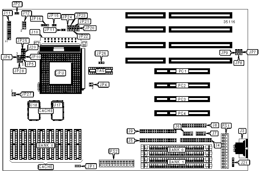
|
Device Type |
Mainboard |
|
Processor |
Pentium/CX 6X86 |
|
Processor Speed |
75/90/100/120/133/150/166MHz |
|
Chip Set |
Intel |
|
Maximum Onboard Memory |
128MB |
|
Cache |
256/512KB |
|
BIOS |
Phoenix |
|
Dimensions |
330mm x 218mm |
|
I/O Options |
32-bit PCI slots (4), floppy drive interface, green PC connector, IDE interfaces (2), parallel port, serial ports (2), VRM connector, PS/2 mouse port, PS/2 keyboard port |
|
NPU Options |
None |
|
CONNECTIONS | |||
|
Function |
Label |
Function |
Label |
|
PS/2 mouse port |
J3 |
Power LED & keylock |
J11 pins 11 - 15 |
|
Floppy drive interface |
J4 |
Speaker |
J11 pins 17 - 20 |
|
IDE interface 2 |
J5 |
Unidentified |
J12 |
|
Serial port 1 |
J6 |
Fan connector |
J20 |
|
Serial port 2 |
J7 |
PS/2 mouse connector |
J21 |
|
Parallel port |
J8 |
IDE interface LED |
JP2 |
|
IDE interface 1 |
J9 |
External battery |
jp16 |
|
VRM connector |
J10 |
32-bit PCI slots |
PC1 - PC4 |
|
Turbo LED |
J11 pins 2 & 3 |
+5V power connection |
PS1 |
|
Green PC connector |
J11 pins 4 & 5 |
+3.3V power connection |
PS2 |
|
Reset switch |
J11 pins 9 & 10 |
|
|
|
USER CONFIGURABLE SETTINGS | |||
|
Setting |
Label |
Position | |
|
|
Normal COM2/4 |
J12 |
Pins 5 & 6, 7 & 8 closed |
|
|
IR function connector |
J12 |
Open |
|
|
Onboard Multi-I/O enabled |
JP7 |
Pins 1 & 2 closed |
|
|
Onboard Multi-I/O disabled |
JP7 |
Pins 2 & 3 closed |
|
? |
CMOS memory normal operation |
JP15 |
Open |
|
|
CMOS memory clear |
JP15 |
Closed |
|
|
Cache type select write back |
JP25 |
Pins 1 & 2 closed |
|
|
Cache type select write through |
JP25 |
Pins 2 & 3 closed |
|
|
PCI clock select PCICLK/4 |
JP26 |
Pins 2 & 3 closed |
|
|
PCI clock select PCICLK/3 |
JP26 |
Pins 1 & 2 closed |
|
DRAM | ||
|
Size |
Bank 0 |
Bank 1 |
|
8MB |
(2) 512K x 36 |
(2) 512K x 36 |
|
8MB |
(2) 1M x 36 |
None |
|
12MB |
(2) 1M x 36 |
(2) 512K x 36 |
|
16MB |
(2) 2M x 36 |
None |
|
16MB |
(2) 1M x 36 |
(2) 1M x 36 |
|
20MB |
(2) 2M x 36 |
(2) 512K x 36 |
|
24MB |
(2) 2M x 36 |
(2) 1M x 36 |
|
32MB |
(2) 4M x 36 |
None |
|
32MB |
(2) 2M x 36 |
(2) 2M x 36 |
|
36MB |
(2) 4M x 36 |
(2) 512K x 36 |
|
40MB |
(2) 4M x 36 |
(2) 1M x 36 |
|
48MB |
(2) 4M x 36 |
(2) 2M x 36 |
|
64MB |
(2) 8M x 36 |
None |
|
64MB |
(2) 4M x 36 |
(2) 4M x 36 |
|
68MB |
(2) 8M x 36 |
(2) 512K x 36 |
|
72MB |
(2) 8M x 36 |
(2) 1M x 36 |
|
80MB |
(2) 8M x 36 |
(2) 2M x 36 |
|
96MB |
(2) 8M x 36 |
(2) 4M x 36 |
|
128MB |
(2) 16M x 36 |
None |
|
128MB |
(2) 8M x 36 |
(2) 8M x 36 |
|
Note: Banks 0/1 are interchangeable. | ||
|
CACHE SIZE | |||
|
Size |
Bank 0 |
U17 & U18 |
TAG |
|
256KB (A) |
None |
(2) 32K x 32 |
(1) 8K x 8 |
|
256KB (B) |
None |
(2) 32K x 32 |
(1) 32K x 8 |
|
256KB (C) |
(8) 32K x 8 |
None |
(1) 8K x 8 |
|
256KB (D) |
(8) 32K x 8 |
None |
(1) 32K x 8 |
|
512KB |
(8) 64K x 8 |
None |
(1) 32K x 8 |
|
CACHE JUMPER | |||||
|
Size |
JP20 |
JP21 |
JP22 |
JP23 |
JP24 |
|
256KB (A & B) |
1 & 2 |
1 & 2 |
1 & 2 |
2 & 3 |
1 & 2 |
|
256KB (C & D) |
1 & 2 |
1 & 2 |
2 & 3 |
2 & 3 |
1 & 2 |
|
512KB |
2 & 3 |
1 & 2 |
2 & 3 |
1 & 2 |
2 & 3 |
|
Note: Pins designated should be in the closed position. | |||||
|
CACHE VOLTAGE | |
|
Setting |
JP1 |
|
Mixed |
Pins 2 & 3 closed |
|
3.3v |
Pins 1 & 2 closed |
|
CPU SPEED (INTEL) | ||||
|
Setting |
Clock Speed |
Multiplier |
J10 |
JP4 |
|
75MHz |
50MHz |
1.5x |
4 & 5, 6 & 7, 19 & 20, 21 & 22 |
Open |
|
90MHz |
60MHz |
1.5x |
4 & 5, 6 & 7, 19 & 20, 21 & 22 |
3 & 4 |
|
100MHz |
66MHz |
1.5x |
4 & 5, 6 & 7, 19 & 20, 21 & 22 |
1 & 2, 3 & 4 |
|
120MHz |
60MHz |
2x |
4 & 5, 6 & 7, 19 & 20, 21 & 22 |
3 & 4 |
|
133MHz |
66MHz |
2x |
4 & 5, 6 & 7, 19 & 20, 21 & 22 |
1 & 2, 3 & 4 |
|
150MHz |
60MHz |
2.5x |
4 & 5, 6 & 7, 19 & 20, 21 & 22 |
3 & 4 |
|
166MHz |
66MHz |
2.5x |
4 & 5, 6 & 7, 19 & 20, 21 & 22 |
1 & 2, 3 & 4 |
|
Note : Numbers designate pins that should be closed. | ||||
|
CPU SPEED (INTEL CON'T) | |||||
|
Setting |
Clock Speed |
Multiplier |
JP5 |
JP10 |
JP11 |
|
75MHz |
50MHz |
1.5x |
Open |
Open |
Open |
|
90MHz |
60MHz |
1.5x |
Open |
Open |
Open |
|
100MHz |
66MHz |
1.5x |
Open |
Open |
Open |
|
120MHz |
60MHz |
2x |
Closed |
Open |
Open |
|
133MHz |
66MHz |
2x |
Closed |
Open |
Open |
|
150MHz |
60MHz |
2.5x |
Closed |
Closed |
Open |
|
166MHz |
66MHz |
2.5x |
Closed |
Closed |
Open |
|
Note : Numbers designate pins that should be closed. | |||||
|
CPU SPEED (CYRIX) | ||||
|
Setting |
Clock Speed |
Multiplier |
J10 |
JP4 |
|
120MHz |
50MHz |
2.5x |
4 & 5, 6 & 7, 19 & 20, 21 & 22 |
Open |
|
133MHz |
55MHz |
2.5x |
4 & 5, 6 & 7, 19 & 20, 21 & 22 |
1 & 2 |
|
150MHz |
60MHz |
2.5x |
4 & 5, 6 & 7, 19 & 20, 21 & 22 |
3 & 4 |
|
166MHz |
66MHz |
2.5x |
4 & 5, 6 & 7, 19 & 20, 21 & 22 |
1 & 2, 3 & 4 |
|
Note : Numbers designate pins that should be closed. | ||||
|
CPU SPEED (CYRIX CON'T) | |||||
|
Setting |
Clock Speed |
Multiplier |
JP5 |
JP10 |
JP11 |
|
120MHz |
50MHz |
2.5x |
Open |
Open |
Open |
|
133MHz |
55MHz |
2.5x |
Open |
Open |
Open |
|
150MHz |
60MHz |
2.5x |
Open |
Open |
Open |
|
166MHz |
66MHz |
2.5x |
Open |
Open |
Open |
|
Note : Numbers designate pins that should be closed. | |||||
|
CPU voltage | |||
|
Setting |
JP6 |
JP27 |
JP50 |
|
3.3v from power supply |
Open |
Open |
N/A |
|
3.3v from VRM (U25 not installed) |
Pins 1 & 2, 3 & 4 closed |
Pins 1 & 2, 3 & 4 closed |
Pins 1 & 2, 3 & 4, 5 & 6, 7 & 8 closed |
|
3.3v from VRM (U25 installed) |
Pins 1 & 2, 3 & 4 closed |
Pins 1 & 2, 3 & 4 closed |
Open |
|
CPU VOLTAGE | |
|
Setting |
JP28 |
|
3.14v - 3.46v |
Pins 1 & 2 closed |
|
3.3v - 3.46v |
Pins 3 & 4 closed |
|
3.45v - 3.6v |
Pins 5 & 6 closed |
|
DMA CHANNEL | ||
|
Setting |
JP8 |
JP9 |
|
DMA1 |
Pins 1 & 2 closed |
Pins 1 & 2 closed |
|
DMA3 |
Pins 2 & 3 closed |
Pins 2 & 3 closed |