CSS LABORATORIES, INC.
MAXSYS 486MTE/VL
|
Processor |
80486SX/80487SX/80486DX/80486DX2/Pentium Overdrive |
|
Processor Speed |
25/33/50(internal)/50/66(internal)MHz |
|
Chip Set |
OPTI |
|
Max. Onboard DRAM |
256MB (128MB on CPU module) |
|
Cache |
64/128/256/512KB |
|
BIOS |
AMI |
|
Dimensions |
330mm x 218mm |
|
I/O Options |
CPU module slot, 32-bit VESA local bus slot (1), floppy drive interface, IDE interface, parallel port, serial ports (2) |
|
NPU Options |
4167 |
|
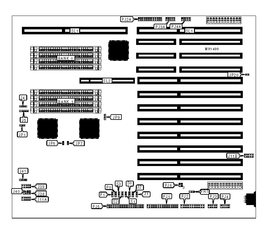
CONNECTIONS |
|||
|
Purpose |
Location |
Purpose |
Location |
|
Speaker |
J4 |
Serial port 2 |
PJ4 |
|
Power LED & keylock |
J5 |
IDE interface |
PJ5 |
|
IDE interface LED |
J38 |
Parallel port (alternate) |
PJ2A |
|
Equipment panel connector |
J39 |
Serial port 1 (alternate) |
PJ3A |
|
IDE interface LED |
J40 |
Serial port 2 (alternate) |
PJ4A |
|
Turbo LED/reset switch |
J41 |
Keyboard connector (alternate) |
J11A |
|
Floppy drive interface |
PJ1 |
Keyboard connector (alternate) |
J11B |
|
Parallel port |
PJ2 |
CPU module slot |
SL1 |
|
Serial port 1 |
PJ3 |
32-bit VESA Local bus slot |
SL2 |
|
Note: The keyboard, parallel and serial connections marked "alternate" are used for easier placement of cables. Do not use a primary and an alternate connection jointly. |
|||
|
USER CONFIGURABLE SETTINGS |
|||
|
Function |
Jumper |
Position |
|
|
» |
On board floppy controller enabled |
J1 |
pins 2 & 3 closed |
|
|
On board floppy controller disabled |
J1 |
pins 1 & 2 closed |
|
» |
On board IDE controller enabled |
J2 |
pins 2 & 3 closed |
|
|
On board IDE controller disabled |
J2 |
pins 1 & 2 closed |
|
» |
CPU bus clock select synchronous |
JP1 |
pins 1 & 2 closed |
|
|
CPU bus clock select asynchronous |
JP1 |
pins 2 & 3 closed |
|
» |
Monitor type select color |
JP9 |
pins 2 & 3 closed |
|
|
Monitor type select monochrome |
JP9 |
pins 1 & 2 closed |
|
|
Factory configured - do not alter |
JP20 |
Open |
|
SERIAL PORT CONFIGURATION |
|||
|
Port 1 |
PJ6 |
S0 |
S1 |
|
Disabled |
N/A |
pins 1 & 2 closed |
pins 1 & 2 closed |
|
COM1 IRQ4 |
pins 1 & 2 closed |
pins 2 & 3 closed |
pins 2 & 3 closed |
|
COM2 IRQ3 |
pins 1 & 3 closed |
pins 1 & 2 closed |
pins 2 & 3 closed |
|
SERIAL PORT CONFIGURATION |
|||
|
Port 2 |
PJ6 |
S2 |
S3 |
|
Disabled |
N/A |
pins 1 & 2 closed |
pins 1 & 2 closed |
|
COM1 IRQ4 |
pins 2 & 4 closed |
pins 1 & 2 closed |
pins 2 & 3 closed |
|
COM2 IRQ3 |
pins 3 & 4 closed |
pins 2 & 3 closed |
pins 2 & 3 closed |
|
PARALLEL PORT CONFIGURATION |
|||
|
Port |
P0 |
P1 |
PRT |
|
Disabled |
pins 1 & 2 closed |
pins 1 & 2 closed |
N/A |
|
LPT 1 IRQ7 |
pins 2 & 3 closed |
pins 1 & 2 closed |
pins 2 & 3 closed |
|
LPT 2 IRQ5 |
pins 2 & 3 closed |
pins 2 & 3 closed |
pins 1 & 2 closed |
|
LPT 3 IRQ 7 |
pins 1 & 2 closed |
pins 2 & 3 closed |
pins 2 & 3 closed |
|
DRAM CONFIGURATION |
||||
|
Size |
Bank 0 |
Bank 1 |
Bank 2 |
Bank 3 |
|
4MB |
(4) 1M x 9 |
NONE |
NONE |
NONE |
|
8MB |
(4) 1M x 9 |
(4) 1M x 9 |
NONE |
NONE |
|
12MB |
(4) 1M x 9 |
(4) 1M x 9 |
(4) 1M x 9 |
NONE |
|
16MB |
(4) 1M x 9 |
(4) 1M x 9 |
(4) 1M x 9 |
(4) 1M x 9 |
|
16MB |
(4) 4M x 9 |
NONE |
NONE |
NONE |
|
20MB |
(4) 1M x 9 |
(4) 4M x 9 |
NONE |
NONE |
|
24MB |
(4) 1M x 9 |
(4) 1M x 9 |
(4) 4M x 9 |
NONE |
|
24MB |
(4) 1M x 9 |
(4) 4M x 9 |
(4) 1M x 9 |
NONE |
|
28MB |
(4) 1M x 9 |
(4) 1M x 9 |
(4) 4M x 9 |
(4) 1M x 9 |
|
28MB |
(4) 1M x 9 |
(4) 4M x 9 |
(4) 1M x 9 |
(4) 1M x 9 |
|
32MB |
(4) 4M x 9 |
(4) 4M x 9 |
NONE |
NONE |
|
36MB |
(4) 1M x 9 |
(4) 4M x 9 |
(4) 4M x 9 |
NONE |
|
36MB |
(4) 4M x 9 |
(4) 4M x 9 |
(4) 1M x 9 |
NONE |
|
40MB |
(4) 1M x 9 |
(4) 1M x 9 |
(4) 4M x 9 |
(4) 4M x 9 |
|
40MB |
(4) 1M x 9 |
(4) 4M x 9 |
(4) 4M x 9 |
(4) 1M x 9 |
|
40MB |
(4) 4M x 9 |
(4) 4M x 9 |
(4) 1M x 9 |
(4) 1M x 9 |
|
48MB |
(4) 4M x 9 |
(4) 4M x 9 |
(4) 4M x 9 |
NONE |
|
52MB |
(4) 1M x 9 |
(4) 4M x 9 |
(4) 4M x 9 |
(4) 4M x 9 |
|
52MB |
(4) 4M x 9 |
(4) 4M x 9 |
(4) 4M x 9 |
(4) 1M x 9 |
|
64MB |
(4) 4M x 9 |
(4) 4M x 9 |
(4) 4M x 9 |
(4) 4M x 9 |
|
64MB |
(4) 16M x 9 |
NONE |
NONE |
NONE |
|
128MB |
(4) 16M x 9 |
(4) 16M x 9 |
NONE |
NONE |
|
196MB |
(4) 16M x 9 |
(4) 16M x 9 |
(4) 16M x 9 |
NONE |
|
256MB |
(4) 16M x 9 |
(4) 16M x 9 |
(4) 16M x 9 |
(4) 16M x 9 |
|
Note: Banks 2 & 3 are located on the CPU module board. |
||||
|
CPU SPEED CONFIGURATION |
||
|
Speed |
JP6 |
JP7 |
|
25MHz |
Open |
Open |
|
33MHz |
Open |
Closed |
|
50iMHz |
Open |
Open |
|
50MHz |
Closed |
Closed |
|
66iMHz |
Open |
Closed |
|
USER CONFIGURABLE SETTINGS |
|||
|
Function |
Jumper |
Position |
|
|
» |
Factory configured - do not alter |
JP8 |
Open |
|
» |
Factory configured - do not alter |
JP77 |
Open |
|
BASE MEMORY CONFIGURATION |
||
|
Memory |
JP20 |
JP21 |
|
384KB |
pins 2 & 3 closed |
Open |
|
512KB |
pins 2 & 3 closed |
Closed |
|
640KB |
pins 1 & 2 closed |
N/A |
|
CACHE CONFIGURATION |
||
|
Size |
Bank 0 |
Bank 1 |
|
64KB |
(4) 8K x 8 |
(4) 8K x 8 |
|
128KB |
(4) 16K x 8 |
(4) 16K x 8 |
|
256KB |
(4) 32K x 8 |
(4) 32K x 8 |
|
512KB |
(4) 64K x 8 |
(4) 64K x 8 |
|
CACHE CONFIGURATION (TAG) |
|||
|
Size |
U55 |
U56 |
U72 |
|
64KB |
(1) 8K x 8 |
NONE |
(1) 16K x 1 or (1) 64K x 1 |
|
128KB |
(1) 8K x 8 |
NONE |
(1) 16K x 1 or (1) 64K x 1 |
|
256KB |
(1) 8K x 8 |
(1) 8K x 8 |
(1) 16K x 1 or (1) 64K x 1 |
|
512KB |
(1) 32K x 8 |
NONE |
(1) 64K x 1 |
|
CACHE JUMPER CONFIGURATION |
|||||||
|
Size |
JP2 |
JP3 |
JP4 |
JP5 |
JP16 |
JP17 |
JP18 |
|
64KB |
2 & 3 |
Open |
Open |
Open |
Open |
Open |
Open |
|
128KB |
1 & 2 |
Closed |
Open |
Open |
Closed |
Open |
Open |
|
256KB |
2 & 3 |
Closed |
Closed |
Open |
Closed |
Closed |
Open |
|
512KB |
1 & 2 |
Closed |
Closed |
Closed |
Closed |
Closed |
Closed |
|
Note: Pins designated should be in the closed position. |
|||||||
|
CPU SPEED CONFIGURATION |
|
|
Speed |
JP12 |
|
25MHz |
pins 2 & 3 closed |
|
33MHz |
pins 2 & 3 closed |
|
50iMHz |
pins 2 & 3 closed |
|
50MHz |
pins 1 & 2 closed |
|
66iMHz |
pins 2 & 3 closed |
|
CPU TYPE CONFIGURATION |
||
|
Type |
JP10 |
JP11 |
|
80486SX |
pins 2 & 3 closed |
Open |
|
80487SX |
pins 1 & 2, 3 & 4 closed |
pins 1 & 2 closed |
|
80486DX/DX2 |
pins 1 & 2, 3 & 4 closed |
pins 2 & 3 closed |
|
Overdrive |
pins 1 & 2, 3 & 4 closed |
pins 1 & 2 closed |