ACER, INC.
486 VESA SYSTEM (VER. 1)
|
Processor |
80486SX/80486DX/80486DX2 |
|
Processor Speed |
20/25/33/40/50(internal)/50/66(internal)MHz |
|
Chip Set |
Unidentified |
|
Video Chip Set |
None |
|
Maximum Onboard Memory |
64MB |
|
Maximum Video Memory |
None |
|
Cache |
128/256KB |
|
BIOS |
Unidentified |
|
Dimensions |
330mm x 218mm |
|
I/O Options |
32-bit VESA local bus slots (2), floppy drive interface, IDE interface, SCSI connector, parallel port, PS/2 mouse port, serial ports (2) |
|
NPU Options |
None |
|
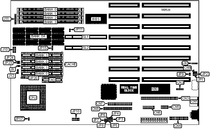
CONNECTIONS | |||
|
Purpose |
Location |
Purpose |
Location |
|
PS/2 mouse port |
CN1 |
IDE interface |
CN8 |
|
HDD/FDD power connector for EPA |
CN2 |
VGA control connector for EPA |
J4 |
|
SCSI interface |
CN3 |
Chassis fan power |
J9 |
|
Parallel port |
CN4 |
Front panel LEDs |
J10 |
|
Serial port 1 |
CN5 |
Auxiliary keyboard/PS/2 mouse |
J11 |
|
Serial port 2 |
CN6 |
IDE interface LED |
J12 |
|
Floppy drive interface |
CN7 |
32-bit VESA local bus slots |
SL1 & SL2 |
|
USER CONFIGURABLE SETTINGS | |||
|
Function |
Label |
Position | |
|
Jumper information unavailable |
CN9 |
Unidentified | |
|
» |
Password check disabled |
JP1 |
Pins 2 & 3 closed |
|
Password check enabled |
JP1 |
Pins 1 & 2 closed | |
|
Jumper information unavailable |
JP2 |
Unidentified | |
|
SCSI IRQ select IRQ10 |
JP3 |
Pins 1 & 2 closed | |
|
SCSI IRQ select IRQ11 |
JP3 |
Pins 2 & 3 closed | |
|
SCSI IRQ disabled |
JP3 |
Open | |
|
» |
Factory configured - do not alter |
JP4 |
Open |
|
» |
Factory configured - do not alter |
JP5 |
Open |
|
SCSI I/O address select 340h - 35Fh |
JP6 |
Open | |
|
SCSI I/O address select 140h - 15Fh |
JP6 |
Closed | |
|
Onboard M5105 disabled |
JP7 |
Open | |
|
Onboard M5105 enabled |
JP7 |
Closed | |
|
» |
Parallel port bidirectional enabled |
JP8 |
Closed |
|
Parallel port bidirectional disabled |
JP8 |
Open | |
|
Battery type select internal |
JP9 |
Closed | |
|
Battery type select external |
JP9 |
Open | |
|
Reset button disabled |
JP23 |
Open | |
|
Reset button enabled |
JP23 |
Closed | |
|
Keylock enabled |
JP24 |
Open | |
|
Keylock disabled |
JP24 |
Closed | |
|
DRAM CONFIGURATION | |||||
|
Size |
Bank 0A |
Bank 0 |
Bank 1 |
Bank 2 |
Bank 3 |
|
4MB |
4MB |
None |
None |
None |
None |
|
8MB |
4MB |
None |
(1) 1M x 36 |
None |
None |
|
12MB |
4MB |
None |
(1) 1M x 36 |
(1) 1M x 36 |
None |
|
16MB (A) |
4MB |
None |
(1) 1M x 36 |
(1) 1M x 36 |
(1) 1M x 36 |
|
16MB (B) |
4MB |
(1) 4M x 36 |
None |
None |
None |
|
20MB |
4MB |
None |
(1) 4M x 36 |
None |
None |
|
24MB |
4MB |
None |
(1) 1M x 36 |
(1) 4M x 36 |
None |
|
32MB |
4MB |
(1) 4M x 36 |
(1) 4M x 36 |
None |
None |
|
36MB |
4MB |
None |
(1) 4M x 36 |
(1) 4M x 36 |
None |
|
40MB |
4MB |
None |
(1) 1M x 36 |
(1) 4M x 36 |
(1) 4M x 36 |
|
48MB |
4MB |
(1) 4M x 36 |
(1) 4M x 36 |
(1) 4M x 36 |
None |
|
64MB |
4MB |
(1) 4M x 36 |
(1) 4M x 36 |
(1) 4M x 36 |
(1) 4M x 36 |
|
Note: If Bank 0 is populated, Bank 0A needs to be disabled with JP15.. | |||||
|
DRAM JUMPER CONFIGURATION | |
|
Size |
JP15 |
|
4MB |
Pins 2 & 3 closed |
|
8MB |
Pins 2 & 3 closed |
|
12MB |
Pins 2 & 3 closed |
|
16MB (A) |
Pins 2 & 3 closed |
|
16MB (B) |
Pins 1 & 2 closed |
|
20MB |
Pins 2 & 3 closed |
|
24MB |
Pins 2 & 3 closed |
|
32MB |
Pins 1 & 2 closed |
|
36MB |
Pins 2 & 3 closed |
|
40MB |
Pins 2 & 3 closed |
|
48MB |
Pins 1 & 2 closed |
|
64MB |
Pins 1 & 2 closed |
|
CACHE CONFIGURATION | |||
|
Size |
Bank 0 |
Bank 1 |
TAG |
|
128KB |
(4) 32K x 8 |
None |
(1) 32K x 8 |
|
256KB |
(4) 32K x 8 |
(4) 32K x 8 |
(1) 32K x 8 |
|
CACHE JUMPER CONFIGURATION | ||
|
Size |
JP17 |
JP20 |
|
128KB |
Open |
Pins 1 & 2 closed |
|
256KB |
Closed |
Pins 2 & 3 closed |
|
CPU SPEED SELECTION | |
|
Speed |
JP10 |
|
20MHz |
Pins 1 & 6 closed |
|
25MHz |
Pins 2 & 7 closed |
|
33MHz |
Pins 3 & 8 closed |
|
40MHz |
Pins 4 & 9 closed |
|
50iMHz |
Pins 2 & 7 closed |
|
50MHz |
Pins 5 & 10 closed |
|
66iMHz |
Pins 3 & 8 closed |
|
VL BUS WAIT STATE SELECTION | ||
|
Setting |
JP11 | |
| » |
0 |
Open |
|
1 |
Closed | |