AT & T
MODEL 6386SX/EL20 (FM-0589-09)
|
Processor |
80386SX (exact location unidentified) |
|
Processor Speed |
20MHz |
|
Chip Set |
Unidentified |
|
Video Chip Set |
None |
|
Maximum Onboard Memory |
32MB |
|
Maximum Video Memory |
None |
|
Cache |
16/32/64KB |
|
BIOS |
Unidentified |
|
Dimensions |
330mm x 218mm |
|
I/O Options |
Floppy drive interface, IDE interface, parallel port, PS/2 mouse port, serial ports (2), VGA feature connector, VGA port, riser slot |
|
NPU Options |
80387SX |
|
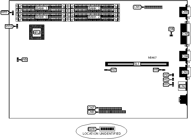
CONNECTIONS | |||
|
Purpose |
Location |
Purpose |
Location |
|
VGA feature connector |
CN1 |
VGA port |
CN6 |
|
PS/2 mouse port |
CN2 |
Floppy drive interface |
CN7 |
|
Serial port |
CN3 |
IDE interface |
CN8 |
|
Serial port |
CN4 |
Riser slot |
SL1 |
|
Parallel port |
CN5 | ||
|
USER CONFIGURABLE SETTINGS | |||
|
Function |
Label |
Position | |
|
» |
16-bit video BIOS enabled |
SW1/3 |
Off |
|
8-bit video BIOS enabled |
SW1/3 |
On | |
|
» |
16-bit video buffer enabled |
SW1/4 |
Off |
|
8-bit video buffer enabled |
SW1/4 |
On | |
|
» |
1024 x 768 interlaced enabled |
SW1/5 |
On |
|
1024 x 768 non interlaced enabled |
SW1/5 |
Off | |
|
» |
On board video enabled |
SW1/8 |
On |
|
On board video disabled |
SW1/8 |
Off | |
|
» |
Password normal operation |
W1 |
Pins 1 & 2 closed |
|
Password clear |
W1 |
Pins 2 & 3 closed | |
|
» |
Factory configured - do not alter |
W2 |
Open |
|
» |
Monitor type select color |
W3 |
Closed |
|
Monitor type select monochrome |
W3 |
Open | |
|
» |
Parallel port unidirectional |
W4 |
Closed |
|
Parallel port bidirectional |
W4 |
Open | |
|
» |
PS/2 mouse IRQ12 enabled |
W5 |
Closed |
|
PS/2 mouse IRQ12 disabled |
W5 |
Open | |
|
» |
Non volatile RAM normal operation |
W7 |
Open |
|
Non volatile RAM clear |
W7 |
Closed | |
|
» |
Speaker type select onboard |
W10 |
Pins 1 & 2 closed |
|
Speaker type select offboard |
W10 |
Pins 2 & 3 closed | |
|
» |
IDE interface LED enabled |
W11 |
Pins 2 & 3 closed |
|
IDE interface LED disabled |
W11 |
Pins 1 & 2 closed | |
|
DRAM CONFIGURATION | ||||
|
Size |
Bank 0 |
Bank 1 |
Bank 2 |
Bank 3 |
|
1MB |
(2) 256K x 9 |
(2) 256K x 9 |
None |
None |
|
1.5MB |
(2) 256K x 9 |
(2) 256K x 9 |
(2) 256K x 9 |
None |
|
2MB |
(2) 256K x 9 |
(2) 256K x 9 |
(2) 256K x 9 |
(2) 256K x 9 |
|
2MB |
(2) 1M x 9 |
None |
None |
None |
|
2.5MB |
(2) 1M x 9 |
(2) 256K x 9 |
None |
None |
|
3MB |
(2) 1M x 9 |
(2) 256K x 9 |
(2) 256K x 9 |
None |
|
3.5MB |
(2) 1M x 9 |
(2) 256K x 9 |
(2) 256K x 9 |
(2) 256K x 9 |
|
4MB |
(2) 1M x 9 |
(2) 1M x 9 |
None |
None |
|
DRAM CONFIGURATION (CON’T) | ||||
|
Size |
Bank 0 |
Bank 1 |
Bank 2 |
Bank 3 |
|
4.5MB |
(2) 1M x 9 |
(2) 1M x 9 |
(2) 256K x 9 |
None |
|
5MB |
(2) 1M x 9 |
(2) 1M x 9 |
(2) 256K x 9 |
(2) 256K x 9 |
|
6MB |
(2) 1M x 9 |
(2) 1M x 9 |
(2) 1M x 9 |
None |
|
6.5MB |
(2) 1M x 9 |
(2) 1M x 9 |
(2) 1M x 9 |
(2) 256K x 9 |
|
8MB |
(2) 1M x 9 |
(2) 1M x 9 |
(2) 1M x 9 |
(2) 1M x 9 |
|
8MB |
(2) 4M x 9 |
None |
None |
None |
|
8.5MB |
(2) 4M x 9 |
(2) 256K x 9 |
None |
None |
|
9MB |
(2) 4M x 9 |
(2) 256K x 9 |
(2) 256K x 9 |
None |
|
9.5MB |
(2) 4M x 9 |
(2) 256K x 9 |
(2) 256K x 9 |
(2) 256K x 9 |
|
10MB |
(2) 4M x 9 |
(2) 1M x 9 |
None |
None |
|
10.5MB |
(2) 4M x 9 |
(2) 1M x 9 |
(2) 256K x 9 |
None |
|
11MB |
(2) 4M x 9 |
(2) 1M x 9 |
(2) 256K x 9 |
(2) 256K x 9 |
|
12MB |
(2) 4M x 9 |
(2) 1M x 9 |
(2) 1M x 9 |
None |
|
12.5MB |
(2) 4M x 9 |
(2) 1M x 9 |
(2) 1M x 9 |
(2) 256K x 9 |
|
14MB |
(2) 4M x 9 |
(2) 1M x 9 |
(2) 1M x 9 |
(2) 1M x 9 |
|
16MB |
(2) 4M x 9 |
(2) 4M x 9 |
None |
None |
|
16.5MB |
(2) 4M x 9 |
(2) 4M x 9 |
(2) 256K x 9 |
None |
|
17MB |
(2) 4M x 9 |
(2) 4M x 9 |
(2) 256K x 9 |
(2) 256K x 9 |
|
18MB |
(2) 4M x 9 |
(2) 4M x 9 |
(2) 1M x 9 |
None |
|
18.5MB |
(2) 4M x 9 |
(2) 4M x 9 |
(2) 1M x 9 |
(2) 256K x 9 |
|
20MB |
(2) 4M x 9 |
(2) 4M x 9 |
(2) 1M x 9 |
(2) 1M x 9 |
|
32MB |
(2) 4M x 9 |
(2) 4M x 9 |
(2) 4M x 9 |
(2) 4M x 9 |
|
CACHE CONFIGURATION | ||
|
Size |
Bank 0 |
Bank 1 |
|
16KB |
(2) 8K x 8 |
None |
|
32KB |
(2) 8K x 8 |
(2) 8K x 8 |
|
64KB |
(2) 32K x 8 |
None |
|
Note: The location of the cache is unidentified. | ||
|
CACHE JUMPER CONFIGURATION | |
|
Size |
W9 |
|
16KB |
Pins 1 & 2 closed |
|
32KB |
Pins 1 & 2 closed |
|
64KB |
Pins 2 & 3 closed |
|
MCLK SELECTION | |||
|
Type |
SW1/6 |
SW1/7 | |
| » |
41.612MHz |
On |
On |
|
36.242MHz |
Off |
On | |
|
37.585MHz |
On |
Off | |
|
44.744MHz |
Off |
Off | |
|
MONITOR SELECTION | |||
|
Setting |
SW1/1 |
SW1/2 | |
| » |
PS/2 VGA |
Off |
Off |
|
MDA |
On |
On | |
|
AT VGA |
Off |
On | |
|
CGA |
On |
Off | |