ATC/UNITRON COMPUTERS & COMPUTER PARTS
MB532
|
Processor |
Pentium |
|
Processor Speed |
75/90/100/120/133MHz |
|
Chip Set |
Intel |
|
Max. Onboard DRAM |
128MB |
|
Cache |
256/512KB |
|
BIOS |
Award |
|
Dimensions |
330mm x 218mm |
|
I/O Options |
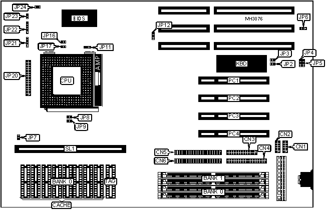
32-bit PCI slots (4), floppy drive interface, green PC connector, IDE interfaces (2), parallel port, serial ports (2), cache slot |
|
NPU Options |
None |
|
CONNECTIONS | |||
|
Purpose |
Location |
Purpose |
Location |
|
Serial port 1 |
CN1 |
VRM module connector |
JP20 |
|
Serial port 2 |
CN2 |
Speaker |
JP21 |
|
Parallel port |
CN3 |
Power LED & keylock |
JP22 |
|
Floppy drive interface |
CN4 |
Reset switch |
JP23 |
|
IDE interface 2 |
CN5 |
Green PC connector |
JP24 |
|
IDE interface 1 |
CN6 |
32-bit PCI slots |
PC1 - PC4 |
|
IDE interface LED |
JP7 |
Cache slot |
SL1 |
|
USER CONFIGURABLE SETTINGS | |||
|
Function |
Jumper |
Position | |
|
» |
CMOS memory normal operation |
JP2 |
Open |
|
CMOS memory clear |
JP2 |
Closed | |
|
» |
BIOS type select EPROM/5v flash |
JP3 |
Open |
|
BIOS type select 12v flash |
JP3 |
Closed | |
|
» |
Factory configured - do not alter |
JP6 |
N/A |
|
AT bus clock select CPU speed/8 |
JP12 |
pins 2 & 3 closed | |
|
AT bus clock select CPU speed/6 |
JP12 |
pins 1 & 2 closed | |
|
DRAM CONFIGURATION | ||
|
Size |
Bank 0 |
Bank 1 |
|
8MB |
(2) 1M x 36 |
NONE |
|
8MB |
NONE |
(2) 1M x 36 |
|
16MB |
(2) 2M x 36 |
NONE |
|
16MB |
NONE |
(2) 2M x 36 |
|
16MB |
(2) 1M x 36 |
(2) 1M x 36 |
|
24MB |
(2) 1M x 36 |
(2) 2M x 36 |
|
24MB |
(2) 2M x 36 |
(2) 1M x 36 |
|
32MB |
(2) 4M x 36 |
NONE |
|
32MB |
NONE |
(2) 4M x 36 |
|
32MB |
(2) 2M x 36 |
(2) 2M x 36 |
|
40MB |
(2) 1M x 36 |
(2) 4M x 36 |
|
40MB |
(2) 4M x 36 |
(2) 1M x 36 |
|
48MB |
(2) 2M x 36 |
(2) 4M x 36 |
|
48MB |
(2) 4M x 36 |
(2) 2M x 36 |
|
64MB |
(2) 8M x 36 |
NONE |
|
64MB |
NONE |
(2) 8M x 36 |
|
64MB |
(2) 4M x 36 |
(2) 4M x 36 |
|
72MB |
(2) 1M x 36 |
(2) 8M x 36 |
|
72MB |
(2) 8M x 36 |
(2) 1M x 36 |
|
80MB |
(2) 2M x 36 |
(2) 8M x 36 |
|
80MB |
(2) 8M x 36 |
(2) 2M x 36 |
|
96MB |
(2) 4M x 36 |
(2) 8M x 36 |
|
96MB |
(2) 8M x 36 |
(2) 4M x 36 |
|
128MB |
(2) 8M x 36 |
(2) 8M x 36 |
|
CACHE CONFIGURATION | |||
|
Size |
Bank 0 |
TAG |
SL1 |
|
256KB (A) |
(8) 32K x 8 |
(1) 8K x 8 |
Not installed |
|
256KB (B) |
NONE |
(1) 8K x 8 |
Installed |
|
512KB (A) |
(8) 64K x 8 |
(1) 16K x 8 |
Not installed |
|
512KB (B) |
NONE |
(1) 16K x 8 |
Installed |
|
Note: The location of Bank 0 and TAG is not exact. It is shown for approximate location purposes only. | |||
|
CPU CLOCK SPEED CONFIGURATION | ||
|
Speed |
JP8 |
JP9 |
|
50MHz |
Closed |
Closed |
|
60MHz |
Open |
Closed |
|
66MHz |
Closed |
Open |
|
CPU INTERNAL CLOCK SPEED CONFIGURATION | ||
|
Speed |
JP16 |
JP17 |
|
1.5x |
Open |
Open |
|
2x |
Closed |
Open |
|
2.5x |
Closed |
Closed |
|
3x |
Open |
Closed |
|
CPU VOLTAGE CONFIGURATION | |
|
Voltage |
JP11 |
|
3.3v |
pins 2 & 3 closed |
|
3.5v |
pins 1 & 2 closed |
|
DMA CONFIGURATION | ||
|
DMA |
JP4 |
JP5 |
|
DMA 1 |
pins 1 & 2 closed |
pins 1 & 2 closed |
|
DMA 3 |
pins 2 & 3 closed |
pins 2 & 3 closed |