ASUS COMPUTER INTERNATIONAL
P/I-P55TP4XE REV 2.1
|
Processor |
Pentium |
|
Processor Speed |
75/90/100/120/133MHz |
|
Chip Set |
SMC |
|
Max. Onboard DRAM |
128MB |
|
Cache |
256/512KB |
|
BIOS |
Award |
|
Dimensions |
254mm x 218mm |
|
I/O Options |
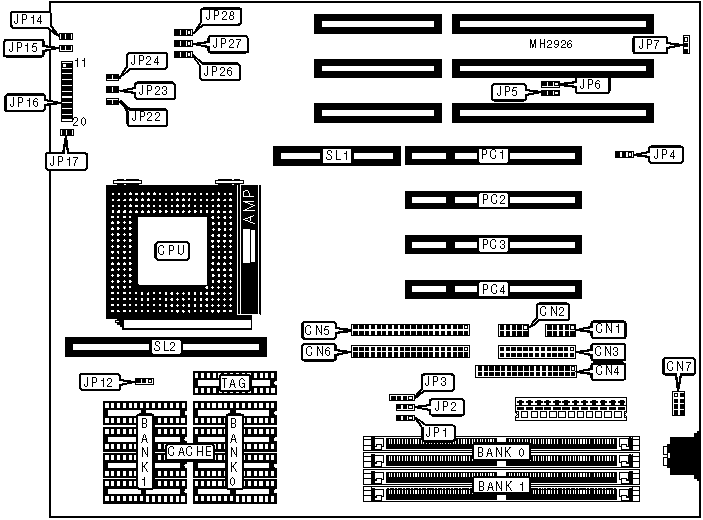
PS/2 mouse port, parallel port, serial ports (2), 32-bit VESA local bus slots (4), green PC connector, floppy drive interface, IDE interfaces (2), Media slot, cache slot |
|
NPU Options |
None |
|
CONNECTIONS |
|||
|
Purpose |
Location |
Purpose |
Location |
|
Serial port 1 |
CN1 |
Power LED & keylock |
JP16 pins 6 - 10 |
|
Serial port 2 |
CN2 |
Reset switch |
JP16 pins 11 & 12 |
|
Parallel port |
CN3 |
Green PC connector |
JP16 pins 16 & 17 |
|
Floppy drive interface |
CN4 |
Turbo LED |
JP16 pins 18 & 19 |
|
IDE interface 1 |
CN5 |
IDE interface LED |
JP17 |
|
IDE interface 2 |
CN6 |
32-bit PCI slots |
PC1 - PC4 |
|
PS/2 mouse interface |
CN7 |
Media slot |
SL1 |
|
Speaker |
JP16 pins 1 - 4 |
External cache card |
SL2 |
|
USER CONFIGURABLE SETTINGS |
|||
|
Function |
Jumper |
Position |
|
|
» |
On board I/O enabled |
JP4 |
pins 1 & 2 closed |
|
|
On board I/O disabled |
JP4 |
pins 2 & 3 closed |
|
» |
PS/2 mouse disabled |
JP7 |
pins 2 & 3 closed |
|
|
PS/2 mouse enabled |
JP7 |
pins 1 & 2 closed |
|
DRAM CONFIGURATION |
||
|
Size |
Bank 0 |
Bank 1 |
|
8MB |
(2) 1M x 36 |
NONE |
|
8MB |
NONE |
(2) 1M x 36 |
|
16MB |
(2) 2M x 36 |
NONE |
|
16MB |
NONE |
(2) 2M x 36 |
|
16MB |
(2) 1M x 36 |
(2) 1M x 36 |
|
24MB |
(2) 1M x 36 |
(2) 2M x 36 |
|
24MB |
(2) 2M x 36 |
(2) 1M x 36 |
|
32MB |
(2) 4M x 36 |
NONE |
|
32MB |
NONE |
(2) 4M x 36 |
|
32MB |
(2) 2M x 36 |
(2) 2M x 36 |
|
40MB |
(2) 1M x 36 |
(2) 4M x 36 |
|
40MB |
(2) 4M x 36 |
(2) 1M x 36 |
|
48MB |
(2) 2M x 36 |
(2) 4M x 36 |
|
48MB |
(2) 4M x 36 |
(2) 2M x 36 |
|
64MB |
(2) 8M x 36 |
NONE |
|
64MB |
NONE |
(2) 8M x 36 |
|
64MB |
(2) 4M x 36 |
(2) 4M x 36 |
|
72MB |
(2) 1M x 36 |
(2) 8M x 36 |
|
72MB |
(2) 8M x 36 |
(2) 1M x 36 |
|
80MB |
(2) 2M x 36 |
(2) 8M x 36 |
|
80MB |
(2) 8M x 36 |
(2) 2M x 36 |
|
96MB |
(2) 4M x 36 |
(2) 8M x 36 |
|
96MB |
(2) 8M x 36 |
(2) 4M x 36 |
|
128MB |
(2) 8M x 36 |
(2) 8M x 36 |
|
CACHE CONFIGURATION |
||||
|
Size |
Bank 0 |
Bank 1 |
TAG |
SL2 |
|
256KB |
(4) 32K x 8 |
(4) 32K x 8 |
(1) 8K, 16K, 32K x 8 |
NONE |
|
256KB |
NONE |
NONE |
NONE |
Card installed |
|
512KB |
(4) 64K x 8 |
(4) 64K x 8 |
(1) 16K, 32K x 8 |
NONE |
|
512KB |
NONE |
NONE |
NONE |
Card installed |
|
CACHE JUMPER CONFIGURATION |
|
|
Size |
JP12 |
|
256KB |
pins 2 & 3 closed |
|
512KB |
pins 1 & 2 closed |
|
CPU SPEED CONFIGURATION |
|||
|
Speed |
JP26 |
JP27 |
JP28 |
|
75MHz |
pins 1 & 2 closed |
pins 2 & 3 closed |
pins 2 & 3 closed |
|
90MHz |
pins 2 & 3 closed |
pins 2 & 3 closed |
pins 1 & 2 closed |
|
100MHz |
pins 2 & 3 closed |
pins 1 & 2 closed |
pins 2 & 3 closed |
|
120MHz |
pins 2 & 3 closed |
pins 2 & 3 closed |
pins 1 & 2 closed |
|
133MHz |
pins 2 & 3 closed |
pins 1 & 2 closed |
pins 2 & 3 closed |
|
CPU SPEED CONFIGURATION |
||
|
Speed |
JP14 |
JP15 |
|
1.5x |
Open |
Open |
|
2x |
Open |
Closed |
|
2.5x |
Closed |
Closed |
|
3x |
Closed |
Open |
|
VOLTAGE REGULATOR CONFIGURATION |
|||
|
Setting |
JP22 |
JP23 |
JP24 |
|
STD/VR |
Closed |
Open |
Open |
|
VRE |
Open |
Closed |
Open |
|
BIOS CONFIGURATION |
||
|
Setting |
JP5 |
JP6 |
|
Normal operation |
pins 1 & 2 closed |
pins 2 & 3 closed |
|
Programming operation |
pins 2 & 3 closed |
pins 2 & 3 closed |
|
SERIAL PORT CONFIGURATION |
|||
|
Setting |
JP1 |
JP2 |
JP3 |
|
COM2 enabled |
pins 1 & 2 closed |
pins 1 & 2 closed |
pins 1 & 2, 3 & 4 closed |
|
Infrared (IR) |
pins 2 & 3 closed |
pins 2 & 3 closed |
pins 2 & 3 closed |