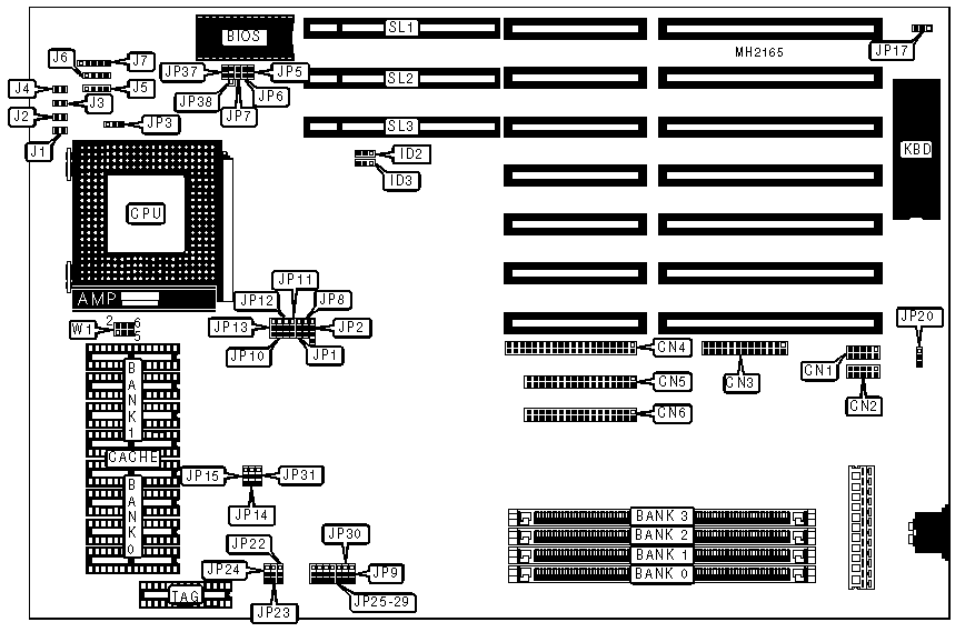
ADVANCED INTEGRATION RESEARCH, INC.
486MI REV. 2.2
|
Processor |
80486SX/80487SX/80486DX/ODP486SX/80486DX2/80486DX4/Pentium Overdrive |
|
Processor Speed |
8/10/12/16/20/25/33/40I/40/50(internal)/60/66(internal)/66MHz |
|
Chip Set |
SIS |
|
Max. Onboard DRAM |
64MB |
|
Cache |
64/128/256/512KB |
|
BIOS |
AMI |
|
Dimensions |
330mm x 218mm |
|
I/O Options |
32-bit VESA local bus slots (3), floppy drive interfaces (2), green PC connector, IDE interface, parallel port, serial ports (2) |
|
NPU Options |
None |
|
CONNECTIONS | |||
|
Purpose |
Location |
Purpose |
Location |
|
Serial port 1 |
CN1 |
Reset switch |
J2 |
|
Serial port 2 |
CN2 |
Turbo switch |
J3 |
|
Parallel port |
CN3 |
Turbo LED |
J4 |
|
IDE interface |
CN4 |
Speaker |
J5 |
|
Floppy drive interface 1 |
CN5 |
IDE interface LED |
J6 |
|
Floppy drive interface 2 |
CN6 |
Power LED & keylock |
J7 |
|
Green PC connector |
J1 |
32-bit VESA local bus slots |
SL1 - SL3 |
|
USER CONFIGURABLE SETTINGS | |||
|
Function |
Jumper |
Position | |
|
» |
Factory configured - do not alter |
JP8 |
pins 1 & 2 closed |
|
» |
Factory configured - do not alter |
JP9 |
pins 1 & 2 closed |
|
» |
Flash BIOS write protect enabled |
JP17 |
pins 1 & 2 closed |
|
Flash BIOS write protect disabled |
JP17 |
pins 2 & 3 closed | |
|
» |
CMOS memory normal operation |
JP20 |
pins 1 & 2 closed |
|
CMOS memory clear |
JP20 |
pins 2 & 3 closed | |
|
» |
VESA IDE interface enabled |
JP22 |
pins 1 & 2 closed |
|
VESA IDE interface disabled |
JP22 |
pins 2 & 3 closed | |
|
» |
Factory configured - do not alter |
JP28 |
Open |
|
» |
Factory configured - do not alter |
JP29 |
Open |
|
» |
Parallel port IRQ select IRQ7 |
JP30 |
pins 1 & 2 closed |
|
Parallel port IRQ select IRQ5 |
JP30 |
pins 2 & 3 closed | |
|
» |
System wake up IRQ select IRQ4 (COM1 & COM2) |
JP31 |
pins 1 & 2 closed |
|
System wake up IRQ select IRQ3 (COM2 & COM4) |
JP31 |
pins 2 & 3 closed | |
|
» |
Factory configured - do not alter |
JP37 |
Open |
|
DRAM CONFIGURATION | ||||
|
Size |
Bank 0 |
Bank 1 |
Bank 2 |
Bank 3 |
|
2MB |
(1) 512K x 36 |
NONE |
NONE |
NONE |
|
4MB |
(1) 512K x 36 |
NONE |
(1) 512K x 36 |
NONE |
|
4MB |
(1) 1M x 36 |
NONE |
NONE |
NONE |
|
6MB |
(1) 512K x 36 |
NONE |
(1) 1M x 36 |
NONE |
|
8MB |
(1) 1M x 36 |
(1) 1M x 36 |
NONE |
NONE |
|
8MB |
(1) 2M x 36 |
NONE |
NONE |
NONE |
|
10MB |
(1) 512K x 36 |
NONE |
(1) 1M x 36 |
(1) 1M x 36 |
|
10MB |
(1) 512K x 36 |
NONE |
(1) 2M x 36 |
NONE |
|
12MB |
(1) 1M x 36 |
(1) 1M x 36 |
(1) 1M x 36 |
NONE |
|
12MB |
(1) 2M x 36 |
NONE |
(1) 1M x 36 |
NONE |
|
16MB |
(1) 4M x 36 |
NONE |
NONE |
NONE |
|
16MB |
(1) 1M x 36 |
(1) 1M x 36 |
(1) 1M x 36 |
(1) 1M x 36 |
|
16MB |
(1) 2M x 36 |
NONE |
(1) 1M x 36 |
(1) 1M x 36 |
|
16MB |
(1) 2M x 36 |
NONE |
(1) 2M x 36 |
NONE |
|
20MB |
(1) 1M x 36 |
(1) 4M x 36 |
NONE |
NONE |
|
24MB |
(1) 1M x 36 |
(1) 1M x 36 |
(1) 4M x 36 |
NONE |
|
24MB |
(1) 2M x 36 |
NONE |
(1) 4M x 36 |
NONE |
|
32MB |
(1) 8M x 36 |
NONE |
NONE |
NONE |
|
32MB |
(1) 4M x 36 |
(1) 4M x 36 |
NONE |
NONE |
|
36MB |
(1) 1M x 36 |
(1) 4M x 36 |
(1) 4M x 36 |
NONE |
|
40MB |
(1) 2M x 36 |
NONE |
(1) 4M x 36 |
(1) 4M x 36 |
|
40MB |
(1) 2M x 36 |
(1) 8M x 36 |
NONE |
NONE |
|
40MB |
(1) 1M x 36 |
(1) 1M x 36 |
(1) 4M x 36 |
(1) 4M x 36 |
|
48MB |
(1) 8M x 36 |
NONE |
(1) 4M x 36 |
NONE |
|
DRAM CONFIGURATION (CON'T) | ||||
|
Size |
Bank 0 |
Bank 1 |
Bank 2 |
Bank 3 |
|
48MB |
(1) 4M x 36 |
(1) 4M x 36 |
(1) 4M x 36 |
NONE |
|
64MB |
(1) 4M x 36 |
(1) 4M x 36 |
(1) 4M x 36 |
(1) 4M x 36 |
|
64MB |
(1) 8M x 36 |
NONE |
(1) 4M x 36 |
(1) 4M x 36 |
|
64MB |
(1) 8M x 36 |
NONE |
(1) 8M x 36 |
NONE |
|
CACHE CONFIGURATION | |||
|
Size |
Bank 0 |
Bank 1 |
TAG |
|
64KB |
(4) 8K x 8 |
(4) 8K x 8 |
(1) 8K x 8 |
|
128KB |
(4) 32K x 8 |
NONE |
(1) 32K x 8 |
|
256KB |
(4) 32K x 8 |
(4) 32K x 8 |
(1) 32K x 8 |
|
512KB |
(4) 128K x 8 |
NONE |
(1) 32K x 8 |
|
CACHE JUMPER CONFIGURATION | ||||||
|
Size |
JP10 |
JP11 |
JP12 |
JP13 |
JP14 |
JP15 |
|
64KB |
1 & 2 |
1 & 2 |
1 & 2 |
2 & 3 |
1 & 2 |
1 & 2 |
|
128KB |
2 & 3 |
1 & 2 |
1 & 2 |
1 & 2 |
1 & 2 |
2 & 3 |
|
256KB |
2 & 3 |
2 & 3 |
1 & 2 |
2 & 3 |
2 & 3 |
2 & 3 |
|
512KB |
2 & 3 |
2 & 3 |
2 & 3 |
1 & 2 |
1 & 2 |
2 & 3 |
|
Note: Pins designated should be in the closed position. | ||||||
|
CPU TYPE CONFIGURATION | |||
|
Type |
JP1 |
JP2 |
JP38 |
|
80486SX |
Open |
pins 2 & 3 closed |
pins 1 & 2 closed |
|
80487SX |
pins 2 & 3 closed |
pins 1 & 2, 3 & 4 closed |
pins 1 & 2 closed |
|
ODP486SX |
pins 2 & 3 closed |
pins 1 & 2, 3 & 4 closed |
pins 1 & 2 closed |
|
80486DX/DX2 |
pins 1 & 2 closed |
pins 1 & 2, 3 & 4 closed |
pins 1 & 2 closed |
|
80486DX4 |
pins 1 & 2 closed |
pins 1 & 2, 3 & 4 closed |
Open |
|
Pentium Overdrive |
pins 2 & 3 closed |
pins 1 & 2, 3 & 4 closed |
pins 1 & 2 closed |
|
CPU CLOCK CONFIGURATION (80486DX4 ONLY) | |||
|
Speed |
External clock speed |
Internal clock speed |
JP3 |
|
3x |
25/33MHz |
75/100MHz |
Open |
|
2.5x |
33MHz |
83MHz |
pins 2 & 3 closed |
|
2x |
50MHz |
100MHz |
pins 1 & 2 closed |
|
CPU SPEED CONFIGURATION | ||||
|
Speed |
JP5 |
JP6 |
JP7 |
ID3 |
|
25MHz |
Closed |
Closed |
Closed |
pins 1 & 2 closed |
|
33MHz |
Closed |
Closed |
Open |
pins 1 & 2 closed |
|
40MHz |
Closed |
Open |
Closed |
pins 2 & 3 closed |
|
50iMHz |
Closed |
Closed |
Closed |
pins 1 & 2 closed |
|
50MHz |
Closed |
Open |
Open |
pins 2 & 3 closed |
|
66iMHz |
Closed |
Closed |
Open |
pins 1 & 2 closed |
|
CPU VOLTAGE CONFIGURATION | |
|
Voltage |
W1 |
|
3.3v |
pins 1 & 3, 2 & 4 closed |
|
5v |
pins 3 & 5, 4 & 6 closed |
|
VESA WAIT STATE CONFIGURATION | |
|
Wait states |
ID2 |
|
0 wait states |
pins 1 & 2 closed |
|
1 wait state |
pins 2 & 3 closed |
|
IDE SPEED CONFIGURATION | ||
|
Speed |
JP23 |
JP24 |
|
0 |
pins 1 & 2 closed |
pins 1 & 2 closed |
|
2 |
pins 2 & 3 closed |
pins 1 & 2 closed |
|
4 |
pins 1 & 2 closed |
pins 2 & 3 closed |
|
6 |
pins 2 & 3 closed |
pins 2 & 3 closed |
|
ECP MODE CONFIGURATION | ||||
|
Setting |
Mode |
JP25 |
JP26 |
JP27 |
|
Enabled |
ECP mode disabled for parallel port |
Open |
Open |
2 & 3 |
|
Disabled |
ECP mode enabled (DMA 3 used) |
1 & 2 |
1 & 2 |
1 & 2 |
|
Disabled |
ECP mode enabled (DMA 1 used) |
2 & 3 |
2 & 3 |
1 & 2 |
|
Note: If setting is enabled- 4 floppy drives are used. Pins designated should be in the closed position. | ||||