DECISION COMPUTER INTERNATIONAL CO., LTD.
8255/8254 LAB CARD
|
Card Type |
Data acquisition |
|
Chip Set |
NEC 8255 |
|
I/O Options |
Digital I/O ports (2) |
|
Data Bus |
8-bit ISA |
|
CONNECTIONS | |||
|
Function |
Label |
Function |
Label |
|
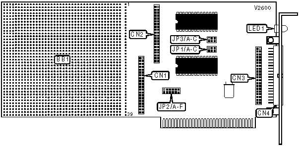
Breadboard (see pinout below) |
BB1 |
Unidentified |
CN3 |
|
Digital I/O port 1 (see pinout below) |
CN1 |
Unidentified |
CN4 |
|
Digital I/O port 2 (see pinout below) |
CN2 | ||
|
BB1 PINOUT | |||
|
Function |
Row |
Function |
Row |
|
Channel 1A bit 7 |
1 |
Channel 1C bit 6 |
21 |
|
Channel 1A bit 6 |
2 |
Channel 1C bit 5 |
22 |
|
Channel 1A bit 5 |
3 |
Channel 1C bit 4 |
23 |
|
Channel 1A bit 4 |
4 |
Channel 1C bit 3 |
24 |
|
Channel 1A bit 3 |
5 |
Channel 1C bit 2 |
25 |
|
Channel 1A bit 2 |
6 |
Channel 1C bit 1 |
26 |
|
Channel 1A bit 1 |
7 |
Channel 1C bit 0 |
27 |
|
Channel 1A bit 0 |
8 |
Not used |
28 |
|
Not used |
9 |
Channel 1B bit 7 |
29 |
|
Clock signal 0 in |
10 |
Channel 1B bit 6 |
30 |
|
Clock signal 1 in |
11 |
Channel 1B bit 5 |
31 |
|
Clock signal 2 in |
12 |
Channel 1B bit 4 |
32 |
|
Gate signal 0 |
13 |
Channel 1B bit 3 |
33 |
|
Gate signal 1 |
14 |
Channel 1B bit 2 |
34 |
|
Gate signal 2 |
15 |
Channel 1B bit 1 |
35 |
|
Clock signal 0 out |
16 |
Channel 1B bit 0 |
36 |
|
Clock signal 1 out |
17 |
Not used |
37 |
|
Clock signal 2 out |
18 |
I/O write register |
38 |
|
Not used |
19 |
I/O read register |
39 |
|
Channel 1C bit 7 |
20 | ||
|
Note:The breadboard is designed to prototype designs. All holes in a given row are electrically connected. Rows marked not used may be utilized by the designer for extra connections. | |||
|
CN1 PINOUT | |||
|
Function |
Pin |
Function |
Pin |
|
Ground |
1 |
Channel 1C bit 6 |
21 |
|
Ground |
2 |
Channel 1C bit 7 |
22 |
|
Ground |
3 |
Channel 1C bit 4 |
23 |
|
Channel 1A bit 3 |
4 |
Channel 1C bit 5 |
24 |
|
Channel 1A bit 1 |
5 |
Channel 1C bit 1 |
25 |
|
Channel 1A bit 2 |
6 |
Channel 1C bit 0 |
26 |
|
Clock signal 0 in |
7 |
Channel 1B bit 7 |
27 |
|
Channel 1A bit 0 |
8 |
Channel 1C bit 2 |
28 |
|
Gate signal 0 |
9 |
Channel 1B bit 6 |
29 |
|
Clock signal 0 out |
10 |
Channel 1C bit 3 |
30 |
|
Clock signal 2 out |
11 |
Channel 1B bit 5 |
31 |
|
Clock signal 2 in |
12 |
Channel 1B bit 0 |
32 |
|
Clock signal 1 in |
13 |
Channel 1B bit 4 |
33 |
|
Gate signal 2 |
14 |
Channel 1B bit 1 |
34 |
|
Clock signal 1 out |
15 |
Channel 1B bit 3 |
35 |
|
Gate signal 1 |
16 |
Channel 1B bit 2 |
36 |
|
Channel 1A bit 5 |
17 |
+5V power |
37 |
|
Channel 1A bit 4 |
18 |
-5V power |
38 |
|
Channel 1A bit 7 |
19 |
+12V power |
39 |
|
Channel 1A bit 6 |
20 |
-12V power |
40 |
|
CN2 PINOUT | |||
|
Function |
Pin |
Function |
Pin |
|
Ground |
1 |
Channel 2C bit 7 |
21 |
|
Ground |
2 |
Channel 2C bit 6 |
22 |
|
Ground |
3 |
Channel 2C bit 5 |
23 |
|
Ground |
4 |
Channel 2C bit 4 |
24 |
|
Ground |
5 |
Channel 2C bit 0 |
25 |
|
Ground |
6 |
Channel 2C bit 1 |
26 |
|
Ground |
7 |
Channel 2C bit 2 |
27 |
|
Ground |
8 |
Channel 2B bit 7 |
28 |
|
Ground |
9 |
Channel 2C bit 3 |
29 |
|
Ground |
10 |
Channel 2B bit 6 |
30 |
|
Ground |
11 |
Channel 2B bit 0 |
31 |
|
Ground |
12 |
Channel 2B bit 5 |
32 |
|
Channel 2A bit 0 |
13 |
Channel 2B bit 1 |
33 |
|
Channel 2A bit 1 |
14 |
Channel 2B bit 4 |
34 |
|
Channel 2A bit 2 |
15 |
Channel 2B bit 2 |
35 |
|
Channel 2A bit 3 |
16 |
Channel 2B bit 3 |
36 |
|
Channel 2A bit 4 |
17 |
+5V power |
37 |
|
Channel 2A bit 5 |
18 |
-5V power |
38 |
|
Channel 2A bit 6 |
19 |
+12V power |
39 |
|
Channel 2A bit 7 |
20 |
-12V power |
40 |
|
USER CONFIGURABLE SETTINGS | |||
|
Setting |
Label |
Position | |
| » |
Counter 0 uses internal clock source |
JP1/A |
Closed |
|
Counter 0 uses external clock source |
JP1/A |
Open | |
| » |
Counter 1 uses internal clock source |
JP1/B |
Closed |
|
Counter 1 uses external clock source |
JP1/B |
Open | |
| » |
Counter 2 uses internal clock source |
JP1/C |
Closed |
|
Counter 2 uses external clock source |
JP1/C |
Open | |
|
BASE I/O ADDRESS | |||||||
|
Setting |
JP2/A |
JP2/B |
JP2/C |
JP2/D |
JP2/E |
JP2/F | |
|
000h |
Closed |
Closed |
Closed |
Closed |
Closed |
Closed | |
|
010h |
Closed |
Closed |
Closed |
Closed |
Closed |
Open | |
|
020h |
Closed |
Closed |
Closed |
Closed |
Open |
Closed | |
|
030h |
Closed |
Closed |
Closed |
Closed |
Open |
Open | |
|
040h |
Closed |
Closed |
Closed |
Open |
Closed |
Closed | |
| » |
2A0h |
Open |
Closed |
Open |
Closed |
Open |
Closed |
|
3B0h |
Open |
Open |
Open |
Closed |
Open |
Open | |
|
3C0h |
Open |
Open |
Open |
Open |
Closed |
Closed | |
|
3D0h |
Open |
Open |
Open |
Open |
Closed |
Open | |
|
3E0h |
Open |
Open |
Open |
Open |
Open |
Closed | |
|
3F0h |
Open |
Open |
Open |
Open |
Open |
Open | |
|
Note: A total of 64 base address settings are available. The jumpers are a binary representation of the decimal memory addresses. JP2/A is the Most Significant Bit and jumper JP2/F is the Least Significant Bit. The jumpers have the following decimal values: JP2/A=512, JP2/B=256, JP2/C=128, JP2/D=64, JP2/E=32, JP2/E=16. Open the jumpers and add the values of the jumpers that are open to obtain the correct memory address. (Open=1, Closed=0) | |||||||
|
WAIT STATES | |||
|
Setting |
JP3/A |
JP3/B |
JP3/C |
|
0 |
Closed |
Open |
Open |
|
1 |
Open |
Closed |
Open |
|
2 |
Open |
Open |
Closed |
|
DIAGNOSTIC LED(S) |
|
The function of the LED is unidentified. |